
Datasheet


TDA8025_1 © NXP B.V. 2009. All rights reserved.
Product data sheet Rev. 01 — 6 April 2009 29 of 38
NXP Semiconductors
TDA8025
IC card interface
[2] To enable the microcontroller to provide the required maximum voltage input level on XTAL1, V
DD(INTF)
must not exceed
V
DD(INTREGD)
+ 0.3 V. See Section 8.1 on page 7 for specific limitations on the maximum V
DD(INTF)
voltage and Table 8 on page 23 for
the limits of XTAL1.
[3] To meet these specifications, V
CC
should be decoupled to pin CGND using two low ESR, ceramic multilayer capacitors one of 470 nF
and one of 220 nF with an ESR of < 100 mΩ.
[4] Using the internal pull-up resistor to V
CC
.
[5] Using the internal pull-up resistor to V
DD(INTF)
.
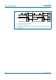
[6] The transition time and the duty factor definitions are shown in Figure 16 on page 30; δ = t1/(t1 + t2).
[7] Pins PRESN and CMDVCCN are active LOW. Pins RSTIN and PRES are active HIGH; see Table 4 on page 12 for pins CLKDIV1 and
CLKDIV2; see Table 5 on page 19 for pins VCC_SEL1 and VCC_SEL2.
[8] If PRESN or PRES is true, the card is considered to be present. A debouncing feature of 4.5 ms typical is built-in.
[9] Pin PRES has an integrated current source to pin GND, pin PRES to V
DD(INTREGD)
; the card is considered as present if at least one of
the two inputs is true.
[10] Pin OFFN is an NMOS drain, using an internal pull-up resistor to V
DD(INTREGD)
.
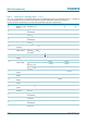
[1] See Figure 8 on page 15.
[2] See Figure 10 on page 16.
[3] See Figure 12 on page 18.
[4] See Figure 15 on page 21.
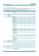
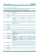
Table 9. Protection characteristics
Symbol Parameter Conditions Min Typ Max Unit
I
CC
supply current shutdown current on
pin V
CC
95 135 185 mA
pin V
CC
135 175 225 mA
pin CLK −70 - +70 mA
pin RST −20 - +20 mA
I
IO
input/output current pins I/O, AUX1 and
AUX2
−15 - +15 mA
T
sd
shutdown temperature - 150 - °C
Table 10. Timing characteristics
Symbol Parameter Conditions Min Typ Max Unit
t
act
activation time total sequence with the crystal oscillator
[1]
35 - 3000 µs
external clock
[2]
35 - 240 µs
t
deact
deactivation time total sequence
[3]
35 80 100 µs
t
d
delay time CLK sent to a card with the crystal oscillator
t
d(start)
= t3
[1]
35 - 3000 µs
t
d(end)
= t5
[1]
160 - 3090 µs
CLK sent to card using an external clock
t
d(start)
= t3
[2]
35 - 150 µs
t
d(end)
=t5
[2]
160 - 240 µs
t
deb
debounce time on pins PRES and PRESN
[4]
3.2 4.5 12 ms