
Datasheet


TDA8025_1 © NXP B.V. 2009. All rights reserved.
Product data sheet Rev. 01 — 6 April 2009 27 of 38
NXP Semiconductors
TDA8025
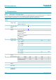
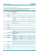
IC card interface
I
OH
HIGH-level
output current
pin I/OUC when active
pull-up; V
OH
= 0.9V
DD
;
C=30pF
−1- - mA
Internal oscillator
f
osc(int)
internal oscillator
frequency
inactive mode 55 140 200 kHz
active mode 1.9 2.7 3.2 MHz
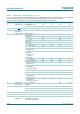
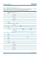
Reset output to the card: pin RST
V
o
output voltage inactive mode
no load 0 - 0.1 V
I
o
= 1 mA - - 0.3 V
I
o
output current when inactive and pin
RST grounded
0- −1mA
t
d
delay time between pins RSTIN and
RST; RST enabled
--2 µs
V
OL
LOW-level output
voltage
I
OL
= 200 µA 0 - 0.2 V
current limit I
OL
= 20 mA V
CC
− 0.4 - V
CC
V
V
OH
HIGH-level
output voltage
I
OH
= −200 µA 0.9V
CC
-V
CC
V
current limit I
OH
= −20 mA 0 - 0.4 V
t
r
rise time C
L
= 100 pF;
V
CC
= 3 V, 1.8 V or 1.2 V
[6]
- - 0.1 µs
t
f
fall time C
L
= 100 pF;
V
CC
= 3 V, 1.8 V or 1.2 V
[6]
- - 0.1 µs
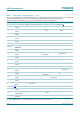
Clock output to the card: pin CLK
V
o
output voltage inactive mode
no load 0 - 0.1 V
I
o
= 1 mA - - 0.3 V
I
o
output current pin CLK when inactive
and grounded
0- −1mA
V
OL
LOW-level output
voltage
I
OL
= 200 µA 0 - 0.3 V
current limit I
OL
=70mA V
CC
− 0.4 - V
CC
V
V
OH
HIGH-level
output voltage
I
OH
= −200 µA 0.9V
CC
-V
CC
V
current limit I
OH
= −70 mA 0 - 0.4 V
t
r
rise time C
L
=30pF
[6]
- - 16 ns
t
f
fall time C
L
=30pF
[6]
- - 16 ns
δ duty cycle except for f
xtal
; C
L
=30pF
[6]
45 - 55 %
SR slew rate rise and fall; C
L
=30pF;
V
CC
= 3 V or 1.8 V
0.2 - - V/ns
C
L
= 30 pF; V
CC
= 1.2 V 0.1 - - V/ns
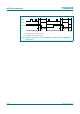
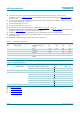
Table 8. Characteristics of IC supply voltage
…continued
T
amb
=25
°
C; all parameters remain within limits but are only statistically tested for the temperature range; f
xtal
= 10 MHz; all
currents flowing into the IC are positive; unless otherwise specified. Parameters specified as a function of
V
DD(INTF)
,V
DDI(REG)
, V
DD(INTREGD)
or V
CC
refer to the actual value at the time of measurement.
Symbol Parameter Conditions Min Typ Max Unit