
Datasheet


TDA8025_1 © NXP B.V. 2009. All rights reserved.
Product data sheet Rev. 01 — 6 April 2009 24 of 38
NXP Semiconductors
TDA8025
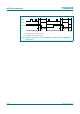
IC card interface
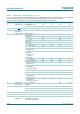
I
L
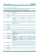
leakage current pin PORADJ < 0.5 V −0.1 +4 +10 µA
pin PORADJ>1V −1- +1 µA
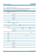
Card supply voltage
[3]
C
dec
decoupling
capacitance
connected to V
CC
550 - 830 nF
V
CC
supply voltage including ripple
inactive mode
no load −0.1 - +0.1 V
I
CC
= 1 mA −0.1 - +0.3 V
active mode
3 V card:
I
CC
< 65 mA DC 2.85 3.05 3.15 V
single current pulse
−100 mA; 2 µs
2.76 3.05 3.20 V
current pulses of
40 nAs at
I
CC
< 200 mA;
t < 400 ns
2.76 3.05 3.20 V
1.8 V card:
I
CC
< 65 mA DC 1.71 1.83 1.89 V
single current pulse
−100 mA; 2 µs
1.66 1.83 1.94 V
current pulses of
15 nAs with I
CC
< 200 mA; t < 400 ns
1.66 1.83 1.94 V
1.2 V card:
I
CC
< 30 mA DC 1.1 1.2 1.3 V
single current pulse
−100 mA; 2 µs
1.1 1.2 1.3 V
current pulses of
15 nAs with I
CC
< 200 mA; t < 400 ns
1.10 1.2 1.3 V
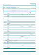
V
ripple(p-p)
peak-to-peak
ripple voltage
pin V
CC
; 20 kHz to
200 MHz
- - 350 mV
I
CC
supply current 0 V to 3 V - - 65 mA
0 V to 1.8 V - - 65 mA
0 V to 1.2 V - - 30 mA
SR slew rate up or down 0.02 0.14 0.26 V/µs
Crystal oscillator: pins XTAL1 and XTAL2
C
ext
external
capacitance
pins XTAL1/XTAL2;
depending on the crystal
or resonator specification
- - 15 pF
Table 8. Characteristics of IC supply voltage
…continued
T
amb
=25
°
C; all parameters remain within limits but are only statistically tested for the temperature range; f
xtal
= 10 MHz; all
currents flowing into the IC are positive; unless otherwise specified. Parameters specified as a function of
V
DD(INTF)
,V
DDI(REG)
, V
DD(INTREGD)
or V
CC
refer to the actual value at the time of measurement.
Symbol Parameter Conditions Min Typ Max Unit