
Datasheet


TDA8025_1 © NXP B.V. 2009. All rights reserved.
Product data sheet Rev. 01 — 6 April 2009 23 of 38
NXP Semiconductors
TDA8025
IC card interface
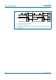
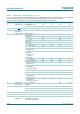
11. Characteristics
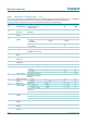
Table 8. Characteristics of IC supply voltage
T
amb
=25
°
C; all parameters remain within limits but are only statistically tested for the temperature range; f
xtal
= 10 MHz; all
currents flowing into the IC are positive; unless otherwise specified. Parameters specified as a function of
V
DD(INTF)
,V
DDI(REG)
, V
DD(INTREGD)
or V
CC
refer to the actual value at the time of measurement.
Symbol Parameter Conditions Min Typ Max Unit
Supply
V
DDI(REG)
regulator input
supply voltage
pin CONFIG = ground 3.6 5 5.5 V
pin CONFIG = V
DDI(REG)
;
regulator is bypassed
3 3.3 3.6 V
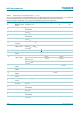
V
DD(INTREGD)
internal
regulated supply
voltage
pin CONFIG = ground
[1]
3 3.3 3.6 V
V
DD(INTF)
interface supply
voltage
pin CONFIG = ground
[2]
1.6 3.0 3.3 V
pin CONFIG = V
DDI(REG)
and V
DD(INTF)
not
connected to V
DDI(REG)
and V
DD(INTREGD)
1.6 3.0 V
DDI(REG)
+ 0.3 V
pin CONFIG = V
DDI(REG)
with V
DD(INTF)
connected
to V
DDI(REG)
and
V
DD(INTREGD)
3 3.3 3.6 V
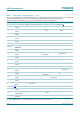
I
DDI(REG)
regulator input
supply current
inactive mode
V
DDI(REG)
=5V
f
xtal
= stopped
- - 300 µA
V
DDI(REG)
=5 V
f
xtal
= 10 MHz;
f
CLK
=
1
⁄
8
f
xtal
- - 2.5 mA
active mode
V
CC
=3V; I
CC
=65mA - - 85 mA
V
CC
= 1.8 V;
I
CC
=65mA
- - 85 mA
V
CC
= 1.2 V;
I
CC
=30mA
- - 50 mA
I
DD(INTF)
interface supply
current
- - 100 µA
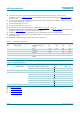
V
th
threshold voltage pin V
DD(INTREGD)
; falling 2.60 2.70 2.80 V
pin V
DD(INTREGD)
; rising 2.65 2.80 2.95 V
pin PORADJ; falling 1.17 1.24 1.31 V
pin PORADJ; rising 1.19 1.26 1.33 V
V
hys
hysteresis
voltage
pin V
DD(INTREGD)
50 100 150 mV
t
w(POR)
power-on reset
pulse width
5 8 18 ms
∆V
th
/∆T threshold voltage
variation with
temperature
- - 0.25 mV/°C