
Datasheet


TDA8025_1 © NXP B.V. 2009. All rights reserved.
Product data sheet Rev. 01 — 6 April 2009 22 of 38
NXP Semiconductors
TDA8025
IC card interface
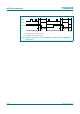
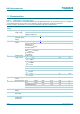
9. Limiting values
Remark: All card contacts are protected against any short-circuit to any other card
contact. Stress beyond the levels indicated in Table 6 can cause permanent damage to
the device. This is a short-term stress rating only and under no circumstances implies
functional operation under long-term stress conditions.
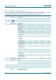
10. Thermal characteristics
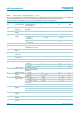
Table 6. Limiting values
In accordance with the Absolute Maximum Rating System (IEC 60134).
Symbol Parameter Conditions Min Max Unit
V
DDI(REG)
regulator input supply voltage −0.3 +5.5 V
V
DD(INTREGD)
internal regulated supply voltage −0.3 +5.5 V
V
I
input voltage pins CMDVCCN, TEST1, TEST2,
CLKDIV2, CLKDIV1, VCC_SEL1,
VCC_SEL2, CONFIG, RSTIN,
OFFN, TEST3, PORADJ, ENCLKIN,
XTAL2, XTAL1, I/OUC, AUX1UC and
AUX2UC
−0.3 +5.5 V
card contact pins PRES, PRESN,
I/O, RST, AUX1, AUX2 and CLK
−0.3 +6.5 V
T
stg
storage temperature −55 +150 °C
P
tot
total power dissipation T
amb
= −25 °C to +85 °C - 0.56 W
T
j
junction temperature - 150 °C
T
amb
ambient temperature −25 +85 °C
V
ESD
electrostatic discharge voltage pins I/O, RST, V
CC
, AUX1, CLK,
AUX2, PRES and PRESN; within
typical application
−6+6kV
Human Body Model (HBM); all pins;
EIA/JESD22-A114-B, June 2000
−2+2kV
Machine Model (MM); all pins;
EIA/JESD22-A115-A, October 1997
−200 +200 V
Charged Device Model (CDM);
all pins, except corner pins −500 +500 V
only corner pins (1, 8, 9, 16, 17,
24, 25 and 32)
−750 +750 V
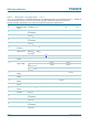
Table 7. Thermal characteristics
Symbol Parameter Conditions Typ Unit
R
th(j-a)
thermal resistance from junction to ambient with exposed pad soldered 42 K/W
without exposed pad soldered 62 K/W