
Datasheet


TDA8025_1 © NXP B.V. 2009. All rights reserved.
Product data sheet Rev. 01 — 6 April 2009 19 of 38
NXP Semiconductors
TDA8025
IC card interface
8.9 V
CC
regulator
The V
CC
buffer is able to continuously deliver up to:
• 65 mA at 3 V
• 65 mA at 1.8 V
• 30 mA at 1.2 V
The V
CC
buffer has an internal overload protection with a threshold value of ±135 mA.
This detection is filtered, enabling spurious current pulses up to 200 mA with a duration of
up to 200 ns to be drawn by the card without causing deactivation. However, the average
current value must be below maximum.
To enhance V
CC
stability, one 470 nF capacitor should be tied to pin CGND near pin 18
and one 220 nF capacitor should be tied to pin CGND near the C1 contact. Both
capacitors should have an ESR < 100 mΩ.
8.10 Fault detection
The following conditions are monitored by the fault detection circuit:
• Short-circuit or high current on pin V
CC
• Card removal during transaction
• V
DD(INTREGD)
falling
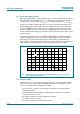
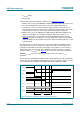
Fig 13. Deactivation sequence with an external clock connected to pin XTAL1
001aai970
CMDVCCN
RST
CLK
I/O
V
CC
XTAL1
OSCINT
t10 t12
t11
t
deact
t13
t14
low frequencyhigh frequency
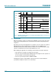
Table 5. Selection of V
CC
using pins VCC_SEL1 and VCC_SEL2
VCC_SEL1 VCC_SEL2 V
CC
003V
0 1 1.8 V
1 0 1.2 V
1 1 1.2 V