
Datasheet


TDA8025_1 © NXP B.V. 2009. All rights reserved.
Product data sheet Rev. 01 — 6 April 2009 17 of 38
NXP Semiconductors
TDA8025
IC card interface
8.7 Active mode
When the activation sequence has finished, the TDA8025 is in active mode. This mode
enables data exchange between the card and the microcontroller using the input and
output lines.
Depending on the layout and application test conditions, line C2 could become polluted
with high frequency noise from line C3. For example, due to an additional 1 pF
capacitance between lines C2/C3 and/or lines C2/C7. It is recommended that a 100 pF
capacitor is added between line C2 and pin CGND, if this occurs.
When building the application, the following recommendations should be adhered to:
• Keep track C3 as far away as possible from other tracks.
• Keep the connection between pin CGND and line C5 straight. The two capacitors on
line C1 should be connected to this ground track.
• Do not use ground loops between CGND and GND.
Following these layout recommendations will ensure that noise remains within the
specifications and jitter on line C3 is less than 100 ps.
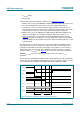
Fig 11. Activation sequence: CLK not controlled by pin RSTIN and with an external clock
connected to pin XTAL1
001aai968
CMDVCCN
XTAL1
V
CC
I/O ATR
CLK
RSTIN
RST
I/OUC
OSCINT
t0 t
d(end)
= t
act
t1 = t2
t
d(start)
t4
low frequency high frequency
> 200 ns