
Datasheet


TDA8025_1 © NXP B.V. 2009. All rights reserved.
Product data sheet Rev. 01 — 6 April 2009 15 of 38
NXP Semiconductors
TDA8025
IC card interface
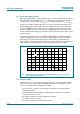
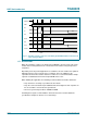
The following sequence occurs when using an external clock connected to pin XTAL1 (see
Figure 10):
1. external clock (XTAL1) started by the microcontroller (t0)
2. CMDVCCN is pulled LOW and the internal oscillator changes to its high frequency (t1)
3. V
CC
rises either from 0 V to 3 V or 0 V to 1.8 V on a controlled slope (t2)
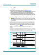
Fig 8. Activation sequence: CLK controlled by pin RSTIN with the crystal oscillator
Fig 9. Activation sequence: CLK not controlled by pin RSTIN with the crystal oscillator
001aai965
CMDVCCN
XTAL
V
CC
I/O ATR
CLK
RSTIN
RST
I/OUC
OSCINT
t0 t
d(end)
= t
act
t1 = t2 t
d(start)
t4
low frequency high frequency
001aai966
CMDVCCN
XTAL
V
CC
I/O ATR
CLK
> 200 ns
RSTIN
RST
I/OUC
OSCINT
t0 t
d(end)
= t
act
t1 = t2
t
d(start)
t4
low frequency high frequency