
Datasheet


TDA8025_1 © NXP B.V. 2009. All rights reserved.
Product data sheet Rev. 01 — 6 April 2009 13 of 38
NXP Semiconductors
TDA8025
IC card interface
8.4 Input and output circuits
When pins I/O and I/OUC are driven HIGH using an 11 kΩ resistor between pins I/O and
V
CC
and/or between pins I/OUC and V
DD(INTF)
, both lines enter the idle state. Pin I/O is
referenced to V
CC
and pin I/OUC to V
DD(INTF)
, thus allowing operation at V
CC
≠ V
DD(INTF)
.
The first side on which a falling edge occurs becomes the master. An anti-latch circuit
disables falling edge detection on the other line, making it the slave. After a time delay
t
d(edge)
, the NMOS transistor on the slave-side is turned on. It then sends logic 0 to the
master-side. When the master returns logic 1, the PMOS transistor on the slave side is
turned on during the time delay (t
pu
). After this sequence, both the master and slave return
to their idle states.
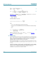
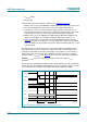
The active pull-up feature ensures fast LOW-to-HIGH transitions making the TDA8025
capable of delivering more than 1 mA, up to an output voltage of 0.9 V
CC
, at a load of
80 pF. At the end of the active pull-up pulse, the output voltage is dependent on the
internal pull-up resistor value and load current. The current sent to and received from the
card’s I/O lines is internally limited to 15 mA at a maximum frequency of 1 MHz.
8.5 Inactive mode
After a power-on reset, the circuit enters the inactive mode, ensuring only the minimum
number of circuits are active while the TDA8025 waits for the microcontroller to start a
session. The inactive mode conditions are as follows:
• all card contacts are inactive. The impedance between the contacts and GND is
approximately 200 Ω.
• pins I/OUC, AUX1UC and AUX2UC are high-impedance using the 11 kΩ pull-up
resistor connected to V
DD(INTF)
• the voltage generators and crystal oscillator are stopped
• the voltage supervisor is active
• the internal oscillator runs in low frequency mode
Fig 7. Output voltage and current on pins I/O, AUX1 and AUX2 as a function of time
during LOW-to-HIGH transitions
t (ns)
0 1008040 6020
001aai964
4
2
6
8
I
OH
I/O
(A)
0
2
1
3
4
V I/O
(V)
0
I
OH
I/O
V I/O