
Datasheet


TDA8025_1 © NXP B.V. 2009. All rights reserved.
Product data sheet Rev. 01 — 6 April 2009 12 of 38
NXP Semiconductors
TDA8025
IC card interface
The duty cycle on pin CLK should be between 45 % and 55 %. To ensure this, the
following must be applied:
• when the CLK frequency is f
xtal
:
If an external clock is connected to pin XTAL1, the duty cycle should be between 48 %
and 52 % with an input signal period transition time of less than 5 %.
If a crystal is used to generate f
xtal
, the duty cycle on pin CLK should be between
45 % and 55 % depending on the layout, crystal characteristics and frequency.
• when CLK frequency is either f
xtal
,
1
⁄
2
f
xtal
,
1
⁄
4
f
xtal
or
1
⁄
8
f
xtal
:
The duty cycle is guaranteed between 45 % and 55 % of the period frequency
divisions.
When a crystal is used, it runs when pin ENCLKIN is driven LOW.
The clock signal is applied to the card based on the activation sequence as shown on the
timing diagrams; see Figure 8 on page 15 to Figure 13 on page 19.
When the signal applied to XTAL1 is controlled by the microcontroller, the clock signal is
sent to the card only after the activation sequence finishes.
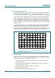
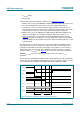
(1) External crystal (optional).
Fig 6. Clock circuits
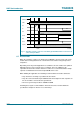
Table 4. Clock configuration
Clock circuitry definition (pins CLKDIV1 and CLKDIV2 can be changed simultaneously; a
>10 XTAL1 period delay is needed. The minimum duration of any CLK state is 10 XTAL1 periods).
CLKDIV1 CLKDIV2 CLK
00
1
⁄
8
f
xtal
01
1
⁄
4
f
xtal
11
1
⁄
2
f
xtal
10f
xtal
001aai963
CLOCK
CIRCUIT
6
5
CLKDIV1
CLKDIV2
ENCLKIN
XTAL
26
27 28
XTAL2
≤ 26 MHz
(1)
XTAL1
15 CLK
MULTIPLEXER
OSCILLATOR