TDA8025 IC card interface Rev. 01 — 6 April 2009 Product data sheet 1. General description The TDA8025 is a cost-effective analog interface for asynchronous smart cards operating at 3 V, 1.8 V or optionally, 1.2 V. Using few external components, the TDA8025 provides integrated supply, protection and control functions for a range of applications. 2. Features n n n n n n n n n n n n n n n Integrated circuit smart card interface 3 V, 1.8 V or 1.
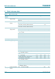
TDA8025 NXP Semiconductors IC card interface 4. Quick reference data Table 1. Symbol Quick reference data Parameter Conditions Min Typ Max Unit regulator input supply voltage pin CONFIG = ground 3.6 5 5.5 V pin CONFIG = VDDI(REG); regulator is bypassed 3 3.3 3.6 V interface supply voltage pin CONFIG = ground 1.6 3.0 3.3 V pin CONFIG = VDDI(REG) and VDD(INTF) not connected to VDDI(REG) and VDD(INTREGD) 1.6 3.0 VDDI(REG) + 0.
TDA8025 NXP Semiconductors IC card interface Table 1. Quick reference data …continued Symbol Parameter Conditions Min Typ Max Unit ICC supply current 0 V to 3 V - - 65 mA 0 V to 1.8 V - - 65 mA 0 V to 1.2 V - - 30 mA slew rate up or down 0.02 0.14 0.26 V/µs tdeact deactivation time total sequence 35 80 100 µs Ptot total power dissipation Tamb = −25 °C to +85 °C - - 0.
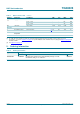
TDA8025 NXP Semiconductors IC card interface 6.
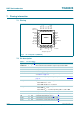
TDA8025 NXP Semiconductors IC card interface 7. Pinning information 25 PORADJ 26 ENCLKIN 27 XTAL2 28 XTAL1 29 I/OUC 30 AUX1UC terminal 1 index area 31 AUX2UC 32 TEST4 7.1 Pinning CMDVCCN 1 24 TEST3 TEST1 2 23 OFFN TEST2 3 22 RSTIN VDD(INTF) 4 CLKDIV2 5 21 VDDI(REG) 20 GND TDA8025 CONFIG 16 PRESN CLK 15 17 RST CGND 14 8 AUX1 13 VCC_SEL2 AUX2 12 19 VDD(INTREGD) 18 VCC I/O 11 7 9 6 PRES 10 CLKDIV1 VCC_SEL1 001aai958 Transparent top view Fig 2.
TDA8025 NXP Semiconductors IC card interface Table 3. Pin description …continued Symbol Pin Type[1] Description CGND 14 G card signal ground CLK 15 O card clock (C3) CONFIG 16 I 3.
TDA8025 NXP Semiconductors IC card interface 8. Functional description Remark: Throughout this document the ISO7816 terminology conventions have been adhered to and it is assumed that the reader is familiar with these. 8.1 Power supplies Two supply selections can be made using pin CONFIG (see Figure 3) depending on the active state of the pin: • pin CONFIG is LOW: supply is pin VDDI(REG). The voltage range of the pin is between 3.6 V and 5.5 V. The regulator output range is between 3 V and 3.6 V.
TDA8025 NXP Semiconductors IC card interface After powering up the device, pin OFFN remains LOW until pins CMDVCCN and PRES are both HIGH or pin CMDVCCN is HIGH and pin PRESN is LOW. During power off, pin OFFN is driven LOW when VDD(INTREGD) is below the falling threshold voltage (Vth). When pin CMDVCCN is HIGH, the internal oscillator frequency (fosc(int)) is switched to Low frequency (inactive) mode to reduce power consumption. 8.2 Voltage supervisors 8.2.
TDA8025 NXP Semiconductors IC card interface 8.2.3 VDD(INTREGD) voltage supervisor with pin PORADJ connected to VDD(INTF) The TDA8025 remains in inactive mode irrespective of the levels on the command lines when • VDD(INTREGD) is less than Vth + Vhys (on pin VDD(INTREGD)) • Pin PORADJ (monitoring VDD(INTF)) is less than Vth + Vhys In both cases, this lasts for the duration of tw(POR) after VDD(INTREGD) (on pin VDD(INTREGD)) and VDD(INTF) (on pin VDD(INTF)) have reached a level higher than Vth + Vhys.
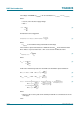
TDA8025 NXP Semiconductors IC card interface The voltage on PORADJ (VPORADJ) can be calculated as: V PORADJ = α × V DD ( INTF ) where: • VDD(INTF) is the interface supply voltage • ratio α 1 α = ---------------R1 1 + ------R2 (2) An activation can be triggered if V th ( max ) V DD ( INTF ) × α > V th ( max ) ⇒ V DD ( INTF ) > -------------------α (3) where • Vth(max) is the maximum rising external threshold voltage The resistance spread of R1 between a minimum value R1min and a maximum value R1max
TDA8025 NXP Semiconductors IC card interface R1 nom ( 1 – β ) V DD ( INTF )actmin --------------- = ----------------- ⋅ ---------------------------------------- – 1 (1 + β) R2 nom V th ( max ) (9) R sum R sum R2 nom = -----------------------------= ------------------------------------------------------------------------------------------R1 nom ( 1 – β ) V DD ( INTF )actmin 1 + ------------- 1 + ----------------- ⋅ ---------------------------------------- – 1 (1 + β) R2 nom V th
TDA8025 NXP Semiconductors IC card interface The duty cycle on pin CLK should be between 45 % and 55 %. To ensure this, the following must be applied: • when the CLK frequency is fxtal: If an external clock is connected to pin XTAL1, the duty cycle should be between 48 % and 52 % with an input signal period transition time of less than 5 %. If a crystal is used to generate fxtal, the duty cycle on pin CLK should be between 45 % and 55 % depending on the layout, crystal characteristics and frequency.
TDA8025 NXP Semiconductors IC card interface 8.4 Input and output circuits When pins I/O and I/OUC are driven HIGH using an 11 kΩ resistor between pins I/O and VCC and/or between pins I/OUC and VDD(INTF), both lines enter the idle state. Pin I/O is referenced to VCC and pin I/OUC to VDD(INTF), thus allowing operation at VCC ≠ VDD(INTF). The first side on which a falling edge occurs becomes the master. An anti-latch circuit disables falling edge detection on the other line, making it the slave.
TDA8025 NXP Semiconductors IC card interface 8.6 Activation sequence After the power-on and internal pulse width delay, the microcontroller checks the presence of the card using signal OFFN. • The card is present when pins OFFN and CMDVCCN are HIGH • The card is not present when pin OFFN is LOW and pin CMDVCCN is HIGH If the card is in the reader (either pin PRESN or pin PRES is true), the microcontroller can start a card session by pulling pin CMDVCCN LOW.
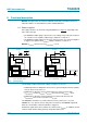
TDA8025 NXP Semiconductors IC card interface CMDVCCN XTAL VCC I/O ATR CLK RSTIN RST I/OUC OSCINT low frequency t0 Fig 8. high frequency t1 = t2 td(start) t4 td(end) = tact 001aai965 Activation sequence: CLK controlled by pin RSTIN with the crystal oscillator CMDVCCN XTAL VCC I/O ATR CLK > 200 ns RSTIN RST I/OUC OSCINT low frequency t0 Fig 9.
TDA8025 NXP Semiconductors IC card interface 4. pins I/O, AUX1 and AUX2 are enabled (t3) 5. CLK is applied to the C3 contact (t4) 6. pin RST is enabled (t5) Calculation of the time delays is as follows: • • • • • t1 = t0 + 2.13 ms t2 = t1 = 3T/2 + 3(1⁄fosc(int)low) t3 = t1 + 5T/2 t4 = driven by the host controller; > t3 and < t5 t5 = t1 + 11T/2 Remark: The value of period T is 64 times the period interval of the internal oscillator (i.e. ±25 µs). t3 is called td(start) and t5 is called td(end).
TDA8025 NXP Semiconductors IC card interface CMDVCCN XTAL1 VCC I/O ATR CLK > 200 ns RSTIN RST I/OUC OSCINT low frequency t0 high frequency t1 = t2 t4 td(start) td(end) = tact 001aai968 Fig 11. Activation sequence: CLK not controlled by pin RSTIN and with an external clock connected to pin XTAL1 8.7 Active mode When the activation sequence has finished, the TDA8025 is in active mode. This mode enables data exchange between the card and the microcontroller using the input and output lines.
TDA8025 NXP Semiconductors IC card interface 8.8 Deactivation sequence When a session is completed, the microcontroller sets pin CMDVCCN to HIGH. The circuit then executes an automatic deactivation sequence by counting the sequencer back to the inactive state (see Figure 12 and Figure 13): 1. pin RST is pulled LOW (t11) 2. the clock is stopped, pin CLK is LOW (t12) 3. pins I/O, AUX1 and AUX2 are pulled LOW (t13) 4. VCC falls to zero (t14).
TDA8025 NXP Semiconductors IC card interface CMDVCCN RST CLK I/O VCC XTAL1 OSCINT high frequency t10 t11 t12 t13 tdeact low frequency t14 001aai970 Fig 13. Deactivation sequence with an external clock connected to pin XTAL1 8.9 VCC regulator Table 5. Selection of VCC using pins VCC_SEL1 and VCC_SEL2 VCC_SEL1 VCC_SEL2 VCC 0 0 3V 0 1 1.8 V 1 0 1.2 V 1 1 1.2 V The VCC buffer is able to continuously deliver up to: • 65 mA at 3 V • 65 mA at 1.8 V • 30 mA at 1.
TDA8025 NXP Semiconductors IC card interface • VDD(INTF) falling • Overheating Fault detection monitors two different situations (see Figure 15 on page 21): 1. Outside card sessions, pin CMDVCCN is HIGH: pin OFFN is LOW if the card is not in the reader and HIGH if the card is in the reader. Any supply voltage drop on VDD(INTREGD) or VDD(INTF) is detected by the supply supervisor. This generates an internal power-on reset pulse but does not act upon the pin OFFN signal.
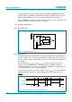
TDA8025 NXP Semiconductors IC card interface PRES OFFN CMDVCCN tdeb tdeb (1) VCC (2) 001aai972 (1) Deactivation caused by card removal. (2) Deactivation caused by short circuit. Fig 15. Operation of debounce feature pin OFFN in combination with pins CMDVCCN, PRES and VCC TDA8025_1 Product data sheet © NXP B.V. 2009. All rights reserved. Rev.
TDA8025 NXP Semiconductors IC card interface 9. Limiting values Remark: All card contacts are protected against any short-circuit to any other card contact. Stress beyond the levels indicated in Table 6 can cause permanent damage to the device. This is a short-term stress rating only and under no circumstances implies functional operation under long-term stress conditions. Table 6. Limiting values In accordance with the Absolute Maximum Rating System (IEC 60134).
TDA8025 NXP Semiconductors IC card interface 11. Characteristics Table 8. Characteristics of IC supply voltage Tamb = 25 °C; all parameters remain within limits but are only statistically tested for the temperature range; fxtal = 10 MHz; all currents flowing into the IC are positive; unless otherwise specified. Parameters specified as a function of VDD(INTF), VDDI(REG), VDD(INTREGD) or VCC refer to the actual value at the time of measurement.
TDA8025 NXP Semiconductors IC card interface Table 8. Characteristics of IC supply voltage …continued Tamb = 25 °C; all parameters remain within limits but are only statistically tested for the temperature range; fxtal = 10 MHz; all currents flowing into the IC are positive; unless otherwise specified. Parameters specified as a function of VDD(INTF), VDDI(REG), VDD(INTREGD) or VCC refer to the actual value at the time of measurement.
TDA8025 NXP Semiconductors IC card interface Table 8. Characteristics of IC supply voltage …continued Tamb = 25 °C; all parameters remain within limits but are only statistically tested for the temperature range; fxtal = 10 MHz; all currents flowing into the IC are positive; unless otherwise specified. Parameters specified as a function of VDD(INTF), VDDI(REG), VDD(INTREGD) or VCC refer to the actual value at the time of measurement.
TDA8025 NXP Semiconductors IC card interface Table 8. Characteristics of IC supply voltage …continued Tamb = 25 °C; all parameters remain within limits but are only statistically tested for the temperature range; fxtal = 10 MHz; all currents flowing into the IC are positive; unless otherwise specified. Parameters specified as a function of VDD(INTF), VDDI(REG), VDD(INTREGD) or VCC refer to the actual value at the time of measurement.
TDA8025 NXP Semiconductors IC card interface Table 8. Characteristics of IC supply voltage …continued Tamb = 25 °C; all parameters remain within limits but are only statistically tested for the temperature range; fxtal = 10 MHz; all currents flowing into the IC are positive; unless otherwise specified. Parameters specified as a function of VDD(INTF), VDDI(REG), VDD(INTREGD) or VCC refer to the actual value at the time of measurement.
TDA8025 NXP Semiconductors IC card interface Table 8. Characteristics of IC supply voltage …continued Tamb = 25 °C; all parameters remain within limits but are only statistically tested for the temperature range; fxtal = 10 MHz; all currents flowing into the IC are positive; unless otherwise specified. Parameters specified as a function of VDD(INTF), VDDI(REG), VDD(INTREGD) or VCC refer to the actual value at the time of measurement.
TDA8025 NXP Semiconductors IC card interface [2] To enable the microcontroller to provide the required maximum voltage input level on XTAL1, VDD(INTF) must not exceed VDD(INTREGD) + 0.3 V. See Section 8.1 on page 7 for specific limitations on the maximum VDD(INTF) voltage and Table 8 on page 23 for the limits of XTAL1. [3] To meet these specifications, VCC should be decoupled to pin CGND using two low ESR, ceramic multilayer capacitors one of 470 nF and one of 220 nF with an ESR of < 100 mΩ.
TDA8025 NXP Semiconductors IC card interface tf tr 90 % VOH 90 % (VOH + VOL)/2 10 % 10 % t1 VOL t2 001aai973 Fig 16. Definition of output and input transition times TDA8025_1 Product data sheet © NXP B.V. 2009. All rights reserved. Rev.
TDA8025 NXP Semiconductors IC card interface 12.
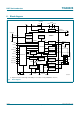
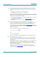
TDA8025 NXP Semiconductors IC card interface VDD(INTF) MICROCONTROLLER VDD(INTF) R1 CMDVCCN TEST1 C5 100 nF PORADJ ENCLKIN XTAL2 XTAL1 I/OUC AUX1UC VDD(INTF) AUX2UC TEST4 VDD(INTF) R2 32 31 30 29 28 27 26 25 1 24 2 23 TEST2 3 VDD(INTF) 4 CLKDIV2 5 CLKDIV1 6 VCC_SEL1 7 VCC_SEL2 8 22 21 TDA8025 20 19 18 17 TEST3 RSTIN VDDI(REG) C1 C6 C2 C7 C3 C8 C4 K2 K1 VCC 10 µF C3 10 µF RST C4 C1 470 nF CONFIG CLK CGND AUX1 AUX2 I/O PRESN PRES C5 C3 GND VDD(INTREGD) 9 10 11
TDA8025 NXP Semiconductors IC card interface 13. Package outline HVQFN32: plastic thermal enhanced very thin quad flat package; no leads; 32 terminals; body 5 x 5 x 0.85 mm A B D SOT617-1 terminal 1 index area A A1 E c detail X C e1 e 1/2 e 16 y y1 C v M C A B w M C b 9 L 17 8 e e2 Eh 1/2 e 1 terminal 1 index area 24 32 25 X Dh 0 2.5 5 mm scale DIMENSIONS (mm are the original dimensions) UNIT A(1) max. A1 b c D (1) Dh E (1) Eh e e1 e2 L v w y y1 mm 1 0.
TDA8025 NXP Semiconductors IC card interface 14. Soldering of SMD packages This text provides a very brief insight into a complex technology. A more in-depth account of soldering ICs can be found in Application Note AN10365 “Surface mount reflow soldering description”. 14.1 Introduction to soldering Soldering is one of the most common methods through which packages are attached to Printed Circuit Boards (PCBs), to form electrical circuits.
TDA8025 NXP Semiconductors IC card interface 14.
TDA8025 NXP Semiconductors IC card interface maximum peak temperature = MSL limit, damage level temperature minimum peak temperature = minimum soldering temperature peak temperature time 001aac844 MSL: Moisture Sensitivity Level Fig 20. Temperature profiles for large and small components For further information on temperature profiles, refer to Application Note AN10365 “Surface mount reflow soldering description”. 15. Abbreviations Table 13.
TDA8025 NXP Semiconductors IC card interface 17. Legal information 17.1 Data sheet status Document status[1][2] Product status[3] Definition Objective [short] data sheet Development This document contains data from the objective specification for product development. Preliminary [short] data sheet Qualification This document contains data from the preliminary specification. Product [short] data sheet Production This document contains the product specification.
TDA8025 NXP Semiconductors IC card interface 19. Contents 1 2 3 4 5 6 7 7.1 7.2 8 8.1 8.2 8.2.1 8.2.2 8.2.3 General description . . . . . . . . . . . . . . . . . . . . . . 1 Features . . . . . . . . . . . . . . . . . . . . . . . . . . . . . . . 1 Applications . . . . . . . . . . . . . . . . . . . . . . . . . . . . 1 Quick reference data . . . . . . . . . . . . . . . . . . . . . 2 Ordering information . . . . . . . . . . . . . . . . . . . . . 3 Block diagram . . . . . . . . . . . . . . . . . . . . . . .