
Datasheet


1999 Apr 07 15
Philips Semiconductors Product specification
Remote 16-bit I/O expander for I
2
C-bus
PCF8575
11 I
2
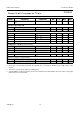
C-BUS TIMING CHARACTERISTICS
See Fig.13 and note 1.
Notes
1. All the timing values are valid within the operating supply voltage and ambient temperature range and refer to V
IL
and V
IH
with an input voltage swing of V
SS
to V
DD
.
2. The device inputs SDA and SCL are filtered and will reject spikes on the bus lines of widths less than t
SW(max)
.
3. The rise and fall times specified here refer to the driver device (PCF8575) and are part of the general fast I
2
C-bus
specification when PCF8575 asserts an acknowledge on SDA, the minimum fall time is 20 ns + 0.1C
b
.
SYMBOL PARAMETER CONDITIONS MIN. MAX. UNIT
f
SCL
SCL clock frequency − 400 kHz
t
SW
tolerable spike width on bus note 2 − 50 ns
t
BUF
BUS free time between a STOP
and START condition
1.3 −µs
t
SU;STA
START condition set-up time 0.6 −µs
t
HD;STA
START condition hold time 0.6 −µs
t
LOW
SCL LOW time 1.3 −µs
t
HIGH
SCL HIGH time 0.6 −µs
t
r
SCL and SDA rise time note 3 20 + 0.1C
b
300 ns
t
f
SCL and SDA fall time note 3 20 + 0.1C
b
300 ns
t
SU;DAT
data set-up time 100 − ns
t
HD;DAT
data hold time 0 − ns
t
SU;STO
STOP condition set-up time 0.6 −µs
C
b
capacitive load represented by
each bus line
− 400 pF
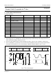
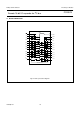
Fig.13 I
2
C-bus timing diagram.
handbook, full pagewidth
PROTOCOL
SCL
SDA
MGL546
BIT 0
LSB
(R/W)
t
SU;STA
t
SU;DAT
t
SU;STO
t
HD;STA
t
HD;DAT
t
BUF
t
r
t
f
t
LOW
t
HIGH
1/f
SCL
START
CONDITION
(S)
BIT 7
MSB
(A7)
BIT 6
(A6)
ACKNOWLEDGE
(A)
STOP
CONDITION
(P)