
Datasheet


PCA9672 All information provided in this document is subject to legal disclaimers. © NXP B.V. 2013. All rights reserved.
Product data sheet Rev. 3 — 27 May 2013 33 of 36
NXP Semiconductors
PCA9672
Remote 8-bit I/O expander for Fm+ I
2
C-bus with interrupt and reset
Modifications:
(continued)
• Section 7.2.2 “Device ID (PCA9672 ID field)”:
– first bullet item following first paragraph changed from “8 bits with the manufacturer name”
to “12 bits with the manufacturer name”
– second bullet item following first paragraph re-written
– List item 6. on page 8
changed from “starting with the 8 manufacturer bits ... , followed by the 13
part identification bits” to “starting with the 12 manufacturer bits ... , followed by the 9 part
identification bits”
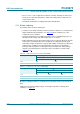
– Figure 10 “PCA9672 Device ID field” updated
– Figure 11
modified: added “Sr” bit (ReSTART condition)
– added paragraph following Figure 11
• Section 8.1 “Quasi-bidirectional I/Os” re-written
• Section 8.2 “Writing to the port (Output mode)” re-written
• Section 8.3 “Reading from a port (Input mode)” re-written
• Section 8.4 “Power-on reset”: second and third sentences re-written
• Section 8.5 “Interrupt output (INT)”: fourth, fifth and sixth paragraphs re-written; added (new) seventh
paragraph
• Section 8.6 “RESET input”: added (new) third sentence
• Section 9.3 “Acknowledge”:
– first paragraph, third sentence re-written
– second paragraph, third sentence re-written
• Section 10.1 “Bidirectional I/O expander applications”:
– second paragraph: second sentence changed from “there is incoming data or a change of data”
to “there has been a change of data”
– added (new) third paragraph
• Added Section 10.2 “How to read and write to I/O expander (example)”
• Section 10.3 “High current-drive load applications”:
– first sentence changed from “maximum sinking current of 25 mA per bit” to “minimum guaranteed
sinking current of 25 mA per bit at 5 V”
– deleted phrase “in the same octal” from second sentence
– appended phrase “which is the device recommended total limit” to fourth sentence
– added (new) fifth sentence
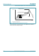
– Figure 21 “
High current-drive load application” modified: added resistors on P6 and P7 signals
• Added Section 10.4 “Migration path”
• Table 6 “Limiting values”: added T
j(max)
limits
• Added Section 12 “Thermal characteristics”
• Table 8 “Static characteristics”:
– sub-section “I/Os; P0 to P7”: added V
IL
characteristic
– sub-section “I/Os; P0 to P7”: added V
IH
characteristic
– sub-section “Input RESET
” is corrected by removing I
OH
row
• Table 9 “Dynamic characteristics”, sub-section “Interrupt timing”:
– symbol/parameter changed from “t
v(D)
, data input valid time” to “t
v(INT)
, valid time on pin INT”
– symbol/parameter changed from t
d(rst)
, reset delay time” to “t
rst(INT)
, reset time on pin INT”
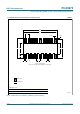
• Added Section 18 “Soldering: PCB footprints”
PCA9672 v.2 20070706 Product data sheet - PCA9672 v.1
PCA9672 v.1 20060620 Objective data sheet - -
Table 13. Revision history …continued
Document ID Release date Data sheet status Change notice Supersedes