
Datasheet


PCA9670 All information provided in this document is subject to legal disclaimers. © NXP B.V. 2013. All rights reserved.
Product data sheet Rev. 3 — 30 May 2013 5 of 35
NXP Semiconductors
PCA9670
Remote 8-bit I/O expander for Fm+ I
2
C-bus with reset
[1] HVQFN16 package die supply ground is connected to both the V
SS
pin and the exposed center pad. The
V
SS
pin must be connected to supply ground for proper device operation. For enhanced thermal, electrical,
and board-level performance, the exposed pad needs to be soldered to the board using a corresponding
thermal pad on the board, and for proper heat conduction through the board thermal vias need to be
incorporated in the PCB in the thermal pad region.
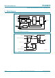
7. Functional description
Refer to Figure 1 “Block diagram of PCA9670”.
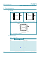
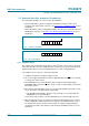
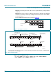
7.1 Device address
Following a START condition, the bus master must send the address of the slave it is
accessing and the operation it wants to perform (read or write). The address format of the
PCA9670 is shown in Figure 6
. Slave address pins AD2, AD1, and AD0 are used to
choose one of 64 slave addresses. These devices can monitor the change in SDA or SCL
in addition to the static levels of V
DD
or V
SS
to decode four states allowing a larger
address range. To conserve power, no internal pull-up resistors are incorporated on AD2,
AD1, or AD0 so they must be externally connected to V
DD
, V
SS
directly or through
resistors, or to SCL or SDA directly. Address values depending on AD2, AD1, and AD0
can be found in Table 4 “
PCA9670 address map”.
Remark: When using the PCA9670, reserved I
2
C-bus addresses must be used with
caution since they can interfere with:
• “reserved for future use” I
2
C-bus addresses (0000 011, 1111 101, 1111 110, 1111 111)
• slave devices that use the 10-bit addressing scheme (1111 0xx)
• High speed mode (Hs-mode) master code (0000 1xx)
The last bit of the first byte defines the operation to be performed. When set to logic 1 a
read is selected, while a logic 0 selects a write operation.
When AD2, AD1 and AD0 are held to V
DD
or V
SS
, the same address as the PCF8574 or
newer PCA8574 is applied.
P7 12 10 quasi-bidirectional I/O 7
RESET
13 11 reset input (active LOW)
SCL 14 12 serial clock line
SDA 15 13 serial data line
V
DD
16 14 supply voltage
Table 3. Pin description
…continued
Symbol Pin Description
SO16, TSSOP16 HVQFN16
Fig 6. PCA9670 address
R/W
002aab636
A6 A5 A4 A3 A2 A1 A0
programmable
slave address