
Datasheet


PCA9670 All information provided in this document is subject to legal disclaimers. © NXP B.V. 2013. All rights reserved.
Product data sheet Rev. 3 — 30 May 2013 3 of 35
NXP Semiconductors
PCA9670
Remote 8-bit I/O expander for Fm+ I
2
C-bus with reset
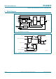
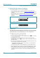
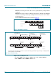
5. Block diagram
Fig 1. Block diagram of PCA9670
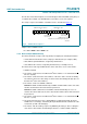
Fig 2. Simplified schematic diagram of P0 to P7
002aac256
RESET
I
2
C-BUS
CONTROL
PCA9670
AD0
AD1
AD2
INPUT
FILTER
SHIFT
REGISTER
SDA
SCL
8 BITS
write pulse
read pulse
POWER-ON
RESET
V
DD
V
SS
I/O
PORT
P0 to P7
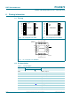
002aah741
write pulse
read pulse
D
CI
S
FF
Q
power-on reset
data from Shift Register
I
trt(pu)
100 µA
I
OH
I
OL
V
DD
P0 to P7
V
SS
D
CI
S
FF
Q
data to Shift Register