
Datasheet

PCA9670 All information provided in this document is subject to legal disclaimers. © NXP B.V. 2013. All rights reserved.
Product data sheet Rev. 3 — 30 May 2013 21 of 35
NXP Semiconductors
PCA9670
Remote 8-bit I/O expander for Fm+ I
2
C-bus with reset
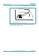
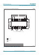
[4] A master device must internally provide a hold time of at least 300 ns for the SDA signal (refer to the V
IL
of the SCL signal) in order to
bridge the undefined region SCL’s falling edge.
[5] The maximum t
f
for the SDA and SCL bus lines is specified at 300 ns. The maximum fall time for the SDA output stage t
f
is specified at
250 ns. This allows series protection resistors to be connected between the SDA and the SCL pins and the SDA/SCL bus lines without
exceeding the maximum specified t
f
.
[6] Input filters on the SDA and SCL inputs suppress noise spikes less than 50 ns.
Rise and fall times refer to V
IL
and V
IH
.
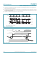
Fig 21. I
2
C-bus timing diagram
002aab175
protocol
START
condition
(S)
bit 7
MSB
(A7)
bit 6
(A6)
bit 0
(R/W)
acknowledge
(A)
STOP
condition
(P)
SCL
SDA
t
HD;STA
t
SU;DAT
t
HD;DAT
t
f
t
BUF
t
SU;STA
t
LOW
t
HIGH
t
VD;ACK
t
SU;STO
1
/ f
SCL
t
r
t
VD;DAT
0.3 × V
DD
0.7 × V
DD
0.3 × V
DD
0.7 × V
DD
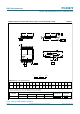
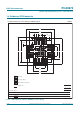
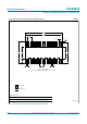
Fig 22. Reset timing
SDA
SCL
002aac018
t
rst
50 %
30 %
50 % 50 %
50 %
t
rec(rst)
t
w(rst)
RESET
IOx_y
output off
START
t
rst
ACK or read cycle