
Datasheet

PCA9670 All information provided in this document is subject to legal disclaimers. © NXP B.V. 2013. All rights reserved.
Product data sheet Rev. 3 — 30 May 2013 13 of 35
NXP Semiconductors
PCA9670
Remote 8-bit I/O expander for Fm+ I
2
C-bus with reset
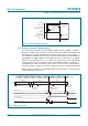
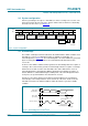
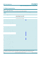
8.3 Reading from a port (Input mode)
The port must have been previously written to logic 1, which is the condition after
power-on reset or hardware reset or software reset. To enter the Read mode the master
(microcontroller) addresses the slave device and sets the last bit of the address byte to
logic 1 (address byte read). The slave will acknowledge and then send the data byte to
the master. The master will NACK and then send the STOP condition or ACK and read the
input register again.
The read of any pin being used as an output will indicate HIGH or LOW depending on the
actual state of the input pin.
If the data on the input port changes faster than the master can read, this data may be
lost. The DATA 2 and DATA 3 are lost because these data did not meet the set-up time
and hold time (see Figure 14
).
8.4 Power-on reset
When power is applied to V
DD
, an internal Power-On Reset (POR) holds the PCA9670 in
a reset condition until V
DD
has reached V
POR
. At that point, the reset condition is released
and the PCA9670 registers and I
2
C-bus/SMBus state machine will initialize to their default
states of all I/Os to inputs with weak current source to V
DD
. Thereafter V
DD
must be
lowered below V
POR
and back up to the operation voltage for power-on reset cycle.
8.5 RESET input
A reset can be accomplished by holding the RESET pin LOW for a minimum of t
w(rst)
. The
PCA9670 registers and I
2
C-bus state machine will be held in their default state until the
RESET
input is once again HIGH. This RESET input pin requires a pull-up resistor to V
DD
if no active connection is used.
A LOW-to-HIGH transition of SDA while SCL is HIGH is defined as the STOP condition (P). Transfer of data can be stopped at
any moment by a STOP condition. When this occurs, data present at the last acknowledge phase is valid (Output mode). Input
data is lost.
Fig 14. Read input port register
A5 A4 A3 A2 A1 A0 1 ASA6
slave address
START condition R/W acknowledge
from slave
002aac266
data from port
A
acknowledge
from master
SDA 1
no acknowledge
from master
read from port
data at port
data from port
DATA 1
DATA 4
DATA 4
DATA 2
DATA 3
P
STOP
condition
t
h(D)
t
su(D)
DATA 1