PCA9670 Remote 8-bit I/O expander for Fm+ I2C-bus with reset Rev. 3 — 30 May 2013 Product data sheet 1. General description The PCA9670 provides general-purpose remote I/O expansion via the two-wire bidirectional I2C-bus (serial clock (SCL), serial data (SDA)). The devices consist of eight quasi-bidirectional ports, 1 MHz 30 mA drive I2C-bus interface, three hardware address inputs and a reset input operating between 2.3 V and 5.5 V.
PCA9670 NXP Semiconductors Remote 8-bit I/O expander for Fm+ I2C-bus with reset ESD protection exceeds 2000 V HBM per JESD22-A114 and 1000 V CDM per JESD22-C101 Latch-up testing is done to JEDEC standard JESD78 which exceeds 100 mA Packages offered: SO16, TSSOP16 and HVQFN16 3. Applications LED signs and displays Servers Keypads Industrial control Medical equipment PLCs Cellular telephones Mobile devices Gaming machines Instrumentation and test measurement 4.
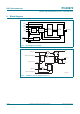
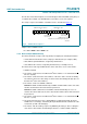
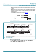
PCA9670 NXP Semiconductors Remote 8-bit I/O expander for Fm+ I2C-bus with reset 5. Block diagram PCA9670 AD0 AD1 AD2 SCL SDA RESET VDD INPUT FILTER I2C-BUS CONTROL SHIFT REGISTER 8 BITS I/O PORT P0 to P7 write pulse read pulse POWER-ON RESET VSS 002aac256 Fig 1. Block diagram of PCA9670 IOH write pulse VDD 100 µA Itrt(pu) data from Shift Register D Q FF IOL CI P0 to P7 S power-on reset VSS D Q FF read pulse CI S data to Shift Register Fig 2.
PCA9670 NXP Semiconductors Remote 8-bit I/O expander for Fm+ I2C-bus with reset 6. Pinning information 6.1 Pinning AD0 1 1 16 VDD 2 16 VDD 15 SDA AD0 AD1 AD1 2 15 SDA AD2 3 14 SCL AD2 3 14 SCL P0 4 13 RESET P0 4 P1 5 12 P7 P1 5 P2 6 11 P6 P2 6 11 P6 P3 7 10 P5 P3 7 10 P5 VSS 8 9 VSS 8 PCA9670D P4 PCA9670PW 12 P7 9 002aac257 P4 002aac258 AD2 1 P0 2 Pin configuration for TSSOP16 13 SDA terminal 1 index area 14 VDD Fig 4.
PCA9670 NXP Semiconductors Remote 8-bit I/O expander for Fm+ I2C-bus with reset Table 3. Symbol Pin description …continued Pin Description SO16, TSSOP16 HVQFN16 P7 12 10 quasi-bidirectional I/O 7 RESET 13 11 reset input (active LOW) SCL 14 12 serial clock line SDA 15 13 serial data line VDD 16 14 supply voltage [1] HVQFN16 package die supply ground is connected to both the VSS pin and the exposed center pad.
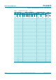
PCA9670 NXP Semiconductors Remote 8-bit I/O expander for Fm+ I2C-bus with reset 7.1.1 Address maps Table 4.
PCA9670 NXP Semiconductors Remote 8-bit I/O expander for Fm+ I2C-bus with reset Table 4.
PCA9670 NXP Semiconductors Remote 8-bit I/O expander for Fm+ I2C-bus with reset 7.2 Software Reset Call, and device ID addresses Two other different addresses can be sent to the PCA9670. • General Call address: allows resetting the PCA9670 through the I2C-bus upon reception of the right I2C-bus sequence. See Section 7.2.1 “Software Reset” for more information. • Device ID address: allows reading ID information from the device (manufacturer, part identification, revision). See Section 7.2.
PCA9670 NXP Semiconductors Remote 8-bit I/O expander for Fm+ I2C-bus with reset The I2C-bus master must interpret a non-acknowledge from the PCA9670 (at any time) as a ‘Software Reset Abort’. The PCA9670 does not initiate a reset of its registers. The unique sequence that initiates a Software Reset is described in Figure 9.
PCA9670 NXP Semiconductors Remote 8-bit I/O expander for Fm+ I2C-bus with reset Remark: The reading of the Device ID can be stopped anytime by sending a NACK command. Remark: If the master continues to ACK the bytes after the third byte, the PCA9670 rolls back to the first byte and keeps sending the Device ID sequence until a NACK has been detected. For the PCA9670, the Device ID is as shown in Figure 10.
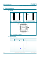
PCA9670 NXP Semiconductors Remote 8-bit I/O expander for Fm+ I2C-bus with reset 8. I/O programming 8.1 Quasi-bidirectional I/O architecture A quasi-bidirectional I/O is an input or output port without using a direction control register. Whenever the master reads the register, the value returned to master depends on the actual voltage or status of the pin. At power-on, all the ports are HIGH with a weak 100 A internal pull-up to VDD but can be driven LOW by an internal transistor, or an external signal.
PCA9670 NXP Semiconductors Remote 8-bit I/O expander for Fm+ I2C-bus with reset VDD input HIGH weak 100 µA current source (inactive when output LOW) pull-up with resistor to VDD or external drive HIGH output HIGH accelerator pull-up P port P7 - P0 pull-down with resistor to VSS or external drive LOW output LOW input LOW VSS 002aah683 Fig 12. Simple quasi-bidirectional I/O 8.
PCA9670 NXP Semiconductors Remote 8-bit I/O expander for Fm+ I2C-bus with reset 8.3 Reading from a port (Input mode) The port must have been previously written to logic 1, which is the condition after power-on reset or hardware reset or software reset. To enter the Read mode the master (microcontroller) addresses the slave device and sets the last bit of the address byte to logic 1 (address byte read). The slave will acknowledge and then send the data byte to the master.
PCA9670 NXP Semiconductors Remote 8-bit I/O expander for Fm+ I2C-bus with reset 9. Characteristics of the I2C-bus The I2C-bus is for 2-way, 2-line communication between different ICs or modules. The two lines are a serial data line (SDA) and a serial clock line (SCL). Both lines must be connected to a positive supply via a pull-up resistor when connected to the output stages of a device. Data transfer may be initiated only when the bus is not busy. 9.
PCA9670 NXP Semiconductors Remote 8-bit I/O expander for Fm+ I2C-bus with reset 9.2 System configuration A device generating a message is a ‘transmitter'; a device receiving is the ‘receiver'. The device that controls the message is the ‘master' and the devices which are controlled by the master are the ‘slaves' (see Figure 17).
PCA9670 NXP Semiconductors Remote 8-bit I/O expander for Fm+ I2C-bus with reset 10. Application design-in information 10.1 Bidirectional I/O expander applications In the 8-bit I/O expander application shown in Figure 19, P0 and P1 are inputs, and P2 to P7 are outputs. When used in this configuration, during a write, the input (P0 and P1) must be written as HIGH so the external devices fully control the input ports.
PCA9670 NXP Semiconductors Remote 8-bit I/O expander for Fm+ I2C-bus with reset { <0100 0001> <1010 0010> //Read PCA9670 data If (P0 == 0) //Temperature sensor activated { // write to PCA9670 with data 0010 1011b to turn on LED (P7), on Switch (P3) and keep P[1:0] as input ports. <0100 0000> <0010 1011> // Write to PCA9670 Exit the loop; } } 10.3 High current-drive load applications The GPIO has a minimum guaranteed sinking current of 25 mA per bit at 5.5 V.
PCA9670 NXP Semiconductors Remote 8-bit I/O expander for Fm+ I2C-bus with reset 11. Limiting values Table 6. Limiting values In accordance with the Absolute Maximum Rating System (IEC 60134). Symbol Parameter VDD supply voltage Conditions Min Max Unit 0.5 +6 V IDD supply current - 100 mA ISS ground supply current - 400 mA VI input voltage VSS 0.5 5.
PCA9670 NXP Semiconductors Remote 8-bit I/O expander for Fm+ I2C-bus with reset 13. Static characteristics Table 8. Static characteristics VDD = 2.3 V to 5.5 V; VSS = 0 V; Tamb = 40 C to +85 C; unless otherwise specified. Symbol Parameter Conditions Min Typ Max Unit Supplies VDD supply voltage 2.3 - 5.
PCA9670 NXP Semiconductors Remote 8-bit I/O expander for Fm+ I2C-bus with reset [3] The value is not tested, but verified on sampling basis. 14. Dynamic characteristics Table 9. Dynamic characteristics VDD = 2.3 V to 5.5 V; VSS = 0 V; Tamb = 40 C to +85 C; unless otherwise specified.
PCA9670 NXP Semiconductors Remote 8-bit I/O expander for Fm+ I2C-bus with reset [4] A master device must internally provide a hold time of at least 300 ns for the SDA signal (refer to the VIL of the SCL signal) in order to bridge the undefined region SCL’s falling edge. [5] The maximum tf for the SDA and SCL bus lines is specified at 300 ns. The maximum fall time for the SDA output stage tf is specified at 250 ns.
PCA9670 NXP Semiconductors Remote 8-bit I/O expander for Fm+ I2C-bus with reset 15. Package outline HVQFN16: plastic thermal enhanced very thin quad flat package; no leads; 16 terminals; body 3 x 3 x 0.85 mm A B D SOT758-1 terminal 1 index area A E A1 c detail X e1 C 1/2 e e 5 y y1 C v M C A B w M C b 8 L 4 9 e e2 Eh 1/2 e 12 1 16 terminal 1 index area 13 Dh X 0 2.5 5 mm scale DIMENSIONS (mm are the original dimensions) UNIT A(1) max.
PCA9670 NXP Semiconductors Remote 8-bit I/O expander for Fm+ I2C-bus with reset SO16: plastic small outline package; 16 leads; body width 7.5 mm SOT162-1 D E A X c HE y v M A Z 9 16 Q A2 A (A 3) A1 pin 1 index θ Lp L 1 8 e detail X w M bp 0 5 10 mm scale DIMENSIONS (inch dimensions are derived from the original mm dimensions) UNIT A max. A1 A2 A3 bp c D (1) E (1) e HE L Lp Q v w y mm 2.65 0.3 0.1 2.45 2.25 0.25 0.49 0.36 0.32 0.23 10.5 10.1 7.6 7.4 1.
PCA9670 NXP Semiconductors Remote 8-bit I/O expander for Fm+ I2C-bus with reset TSSOP16: plastic thin shrink small outline package; 16 leads; body width 4.4 mm SOT403-1 E D A X c y HE v M A Z 9 16 Q (A 3) A2 A A1 pin 1 index θ Lp L 1 8 e detail X w M bp 0 2.5 5 mm scale DIMENSIONS (mm are the original dimensions) UNIT A max. A1 A2 A3 bp c D (1) E (2) e HE L Lp Q v w y Z (1) θ mm 1.1 0.15 0.05 0.95 0.80 0.25 0.30 0.19 0.2 0.1 5.1 4.9 4.5 4.3 0.65 6.
PCA9670 NXP Semiconductors Remote 8-bit I/O expander for Fm+ I2C-bus with reset 16. Handling information All input and output pins are protected against ElectroStatic Discharge (ESD) under normal handling. When handling ensure that the appropriate precautions are taken as described in JESD625-A or equivalent standards. 17. Soldering of SMD packages This text provides a very brief insight into a complex technology.
PCA9670 NXP Semiconductors Remote 8-bit I/O expander for Fm+ I2C-bus with reset • Process issues, such as application of adhesive and flux, clinching of leads, board transport, the solder wave parameters, and the time during which components are exposed to the wave • Solder bath specifications, including temperature and impurities 17.
PCA9670 NXP Semiconductors Remote 8-bit I/O expander for Fm+ I2C-bus with reset temperature maximum peak temperature = MSL limit, damage level minimum peak temperature = minimum soldering temperature peak temperature time 001aac844 MSL: Moisture Sensitivity Level Fig 26. Temperature profiles for large and small components For further information on temperature profiles, refer to Application Note AN10365 “Surface mount reflow soldering description”.
PCA9670 NXP Semiconductors Remote 8-bit I/O expander for Fm+ I2C-bus with reset 18. Soldering: PCB footprints Footprint information for reflow soldering of HVQFN16 package SOT758-1 Hx Gx D P 0.025 0.025 C (0.105) SPx Hy SPy tot nSPx Gy SPy nSPy SLy By Ay SPx tot SLx Bx Ax solder land solder paste deposit solder land plus solder paste occupied area nSPx nSPy 2 2 Dimensions in mm P Ax Ay Bx By C D SLx SLy 0.50 4.00 4.00 2.20 2.20 0.90 0.24 1.50 1.
PCA9670 NXP Semiconductors Remote 8-bit I/O expander for Fm+ I2C-bus with reset Footprint information for reflow soldering of SO16 package SOT162-1 Hx Gx P2 (0.125) Hy Gy (0.125) By Ay C D2 (4x) D1 P1 Generic footprint pattern Refer to the package outline drawing for actual layout solder land occupied area DIMENSIONS in mm P1 1.270 P2 Ay 1.320 11.200 By C D1 D2 6.400 2.400 0.700 Gx 0.800 10.040 Gy Hx Hy 8.600 11.900 11.450 sot162-1_fr Fig 28.
PCA9670 NXP Semiconductors Remote 8-bit I/O expander for Fm+ I2C-bus with reset Footprint information for reflow soldering of TSSOP16 package SOT403-1 Hx Gx P2 (0.125) Hy Gy (0.125) By Ay C D2 (4x) D1 P1 Generic footprint pattern Refer to the package outline drawing for actual layout solder land occupied area DIMENSIONS in mm P1 P2 Ay By C D1 D2 Gx Gy Hx Hy 0.650 0.750 7.200 4.500 1.350 0.400 0.600 5.600 5.300 5.800 7.450 sot403-1_fr Fig 29.
PCA9670 NXP Semiconductors Remote 8-bit I/O expander for Fm+ I2C-bus with reset 19. Abbreviations Table 12.
PCA9670 NXP Semiconductors Remote 8-bit I/O expander for Fm+ I2C-bus with reset Table 13. Revision history …continued Document ID Modifications: (continued) Release date • • • • • • • • Data sheet status Change notice Supersedes Section 8.1 “Quasi-bidirectional I/O architecture” re-written Section 8.2 “Writing to the port (Output mode)”, first paragraph: first, second and third sentences re-written Figure 13 “Write mode (output)” updated Section 8.
PCA9670 NXP Semiconductors Remote 8-bit I/O expander for Fm+ I2C-bus with reset 21. Legal information 21.1 Data sheet status Document status[1][2] Product status[3] Definition Objective [short] data sheet Development This document contains data from the objective specification for product development. Preliminary [short] data sheet Qualification This document contains data from the preliminary specification.
PCA9670 NXP Semiconductors Remote 8-bit I/O expander for Fm+ I2C-bus with reset Export control — This document as well as the item(s) described herein may be subject to export control regulations. Export might require a prior authorization from competent authorities. Non-automotive qualified products — Unless this data sheet expressly states that this specific NXP Semiconductors product is automotive qualified, the product is not suitable for automotive use.
PCA9670 NXP Semiconductors Remote 8-bit I/O expander for Fm+ I2C-bus with reset 23. Contents 1 2 3 4 4.1 5 6 6.1 6.2 7 7.1 7.1.1 7.2 7.2.1 7.2.2 8 8.1 8.2 8.3 8.4 8.5 9 9.1 9.1.1 9.2 9.3 10 10.1 10.2 10.3 10.4 11 12 13 14 15 16 17 17.1 17.2 17.3 17.4 18 General description . . . . . . . . . . . . . . . . . . . . . . 1 Features and benefits . . . . . . . . . . . . . . . . . . . . 1 Applications . . . . . . . . . . . . . . . . . . . . . . . . . . . . 2 Ordering information . . . . . . . . . . . . . . . .