
Datasheet

PCA9646 All information provided in this document is subject to legal disclaimers. © NXP B.V. 2011. All rights reserved.
Product data sheet Rev. 1 — 1 March 2011 8 of 22
NXP Semiconductors
PCA9646
Buffered 4-channel 2-wire bus switch
[1] Supply voltage dependent; refer to graphs (Figure 9 through Figure 12) for typical trend.
[2] Guaranteed by design, not subject to test.
RESET
V
IH
HIGH-level input voltage V
DD
= 2.7 V 2.0 - - V
V
DD
= 5.5 V 4.8 - - V
V
IL
LOW-level input voltage V
DD
= 2.7 V - - 650 mV
V
DD
= 5.5 V - - 900 mV
V
hys
hysteresis voltage V
DD
=2.7V 100 - - mV
V
DD
=5.5V 200 - - mV
I
LI
input leakage current pin at V
DD
or V
SS
1- +1 A
t
w(rst)L
LOW-level reset time V
I
<V
IL
[2]
-25- ns
t
rst
reset time RESET pin; from V
I
> V
IH
- 250 500 ns
t
POR
power-on reset pulse time RESET pin; from V
I
> V
IH
- 250 500 ns
Address pins (A0, A1, A2)
V
IH
HIGH-level input voltage V
DD
= 2.7 V 1.7 - - V
V
DD
= 5.5 V 3.5 - - V
V
IL
LOW-level input voltage V
DD
=2.7V --0.7V
V
DD
=5.5V --1.5V
I
LI
input leakage current pin at V
DD
or V
SS
1- +1 A
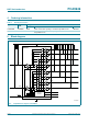
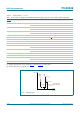
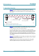
Timing characteristics (Figure 8
)
t
d
delay time R
PU
= 200 ; V
DD
= 2.7 V - 100 - ns
R
PU
= 200 ; V
DD
=5.5V - 70 - ns
t
f
fall time R
PU
= 200 -16- ns
Table 4. Characteristics
…continued
T
amb
=
40
C to +85
C; voltages are specified with respect to ground (V
SS
); V
DD
= 5.5 V unless otherwise specified.
Symbol Parameter Conditions Min Typ Max Unit
Fig 8. Timing diagram
002aaf438
t
f
t
d
V
I2C-bus
time
70 % V
DD
30 % V
DD
SDx, SCx input
SDx, SCx output
V
IL