
Datasheet

PCA9646 All information provided in this document is subject to legal disclaimers. © NXP B.V. 2011. All rights reserved.
Product data sheet Rev. 1 — 1 March 2011 7 of 22
NXP Semiconductors
PCA9646
Buffered 4-channel 2-wire bus switch
9. Limiting values
[1] Voltages are specified with respect to pin 8 (V
SS
).
10. Characteristics
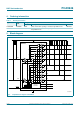
Table 3. Limiting values
In accordance with the Absolute Maximum Rating System (IEC 60134).
Symbol Parameter Conditions Min Max Unit
V
DD
supply voltage
[1]
0.3 +7 V
V
I/O
voltage on an input/output pin pins SDx, SCx
[1]
V
SS
0.5 +7 V
V
I
input voltage RESET pin
[1]
V
SS
0.5 V
DD
+0.5 V
address pins A2, A1, A0
[1]
V
SS
0.5 V
DD
+0.5 V
I
I
input current pins other than SCx/SDx - 20 mA
all SCx and SDx - 40 mA
I
SS
ground supply current - 280 mA
P
tot
total power dissipation - 300 mW
T
stg
storage temperature 55 +125 C
T
amb
ambient temperature operating 40 +85 C
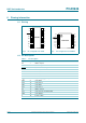
Table 4. Characteristics
T
amb
=
40
C to +85
C; voltages are specified with respect to ground (V
SS
); V
DD
= 5.5 V unless otherwise specified.
Symbol Parameter Conditions Min Typ Max Unit
Power supply
V
DD
supply voltage operating 2.7 - 5.5 V
I
DD
supply current quiescent; V
I
(RESET pin)=0V--1 A
I
2
C-bus ports (SCL, SDA, SC[3:0], SD[3:0])
V
I2C-bus
I
2
C-bus voltage SDx, SCx - - 5.5 V
V
IL
LOW-level input voltage V
DD
=2.7V
[1]
--0.4V
V
DD
=5.5V
[1]
--0.5V
V
IH
HIGH-level input voltage V
DD
=2.7V
[1]
1.2 - - V
V
DD
=5.5V
[1]
2.0 - - V
V
I(hys)
hysteresis of input voltage V
DD
=2.7V
[1]
80 - - mV
V
DD
=5.5V
[1]
200 - - mV
I
LI
input leakage current pin at V
DD
or V
SS
1- +1 A
I
O(sink)
output sink current LOW-level; V
Sxx
input < V
IL
30 - - mA
V
OL
LOW-level output voltage I
OL
=30mA; V
DD
= 2.7 V - 260 450 mV
I
OL
=30mA; V
DD
= 5.5 V - 140 275 mV
Pins SDA, SD0, SD1, SD2, SD3
V
lock
direction lock voltage V
DD
=2.7V
[1]
--1.3V
V
DD
=5.5V
[1]
--3.0V
V
unlock
direction unlock voltage V
DD
=2.7V
[1]
2.0 - - V
V
DD
=5.5V
[1]
4.8 - - V