
Datasheet

PCA9646 All information provided in this document is subject to legal disclaimers. © NXP B.V. 2011. All rights reserved.
Product data sheet Rev. 1 — 1 March 2011 6 of 22
NXP Semiconductors
PCA9646
Buffered 4-channel 2-wire bus switch
A LOW or ‘zero’ bit (B[3:0]) indicates that the respective channel (SC[3:0], SD[3:0]) is
disabled. The default reset condition of the register is all zeros, all channels disabled,
forward direction. A HIGH or ‘one’ bit indicates the respective channel is enabled.
Example: B3 = 1, B2 = 0, B1 = 1, B0 = 0 means channel 3 (SC3/SD3) and channel 1
(SC1/SD1) are enabled, and channel 2 (SC2/SD2) and channel 0 (SC0/SD0) are
disabled.
As each channel is individually buffered, the loads on each are isolated, and therefore
there is no special requirement to keep the sum of the collective capacitances below the
maximum bus capacitance. Instead, each line may have up to the maximum bus
capacitance and be enabled or disabled without affecting the performance of the other
channels.
The Most Significant Bit (MSB) B7 is used to set the direction of the SCL (clock) signal.
The default state is LOW (zero). In this state, the SCL port will act as the input, and the IC
will supply a buffered signal to any of the four output channels (SC0 to SC3) which are
enabled. When B7 is set HIGH (one), the clock signal direction is reversed. The ports
SC0 to SC3 act as inputs, the ANDed combination of the selected signals is buffered and
output on the SCL pin.
The PCA9646 is always addressable from the SCL/SDA side, regardless of the state of
B7. Any device which can communicate data to the SCL/SDA pins, either by being directly
attached to those pins or by transmitting through the PCA9646 (when B7 = 1), may
address the device and change the control register’s contents. The Control register is only
updated upon receipt of the STOP condition.
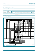
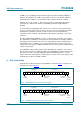
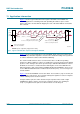
8. Bus transaction
A typical I
2
C-bus write transaction to the PCA9646 is shown in Figure 6. A typical read
transaction is shown in Figure 7
.
Fig 6. PCA9646 write transaction to Control register
Fig 7. PCA9646 read transaction from Control register
002aaf370
S 1 1 1 0 A2 A1 A0
slave address
0 A B7 X X X B3 B2 B1 B0 A P
Control register
START
condition
R/W acknowledge
from slave
acknowledge
from slave
STOP
condition
002aaf371
S 1 1 1 0 A2 A1 A0
slave address
1 A B7 0 0 0 B3 B2 B1 B0 NA P
Control register
START
condition
R/W acknowledge
from slave
not acknowledge
from master
STOP
condition