
Datasheet

PCA9646 All information provided in this document is subject to legal disclaimers. © NXP B.V. 2011. All rights reserved.
Product data sheet Rev. 1 — 1 March 2011 5 of 22
NXP Semiconductors
PCA9646
Buffered 4-channel 2-wire bus switch
7.5 RESET — reset IC to default state
The active LOW RESET input is used to disable the buffer, and reset it to its default state.
The IC should only be disabled when the bus is idle to avoid truncation of commands
which may confuse other devices on the bus.
The RESET
signal will clear the contents of the Control register, which has the effect of
disabling all output lines SC[0:3] and SD[0:3]. It is the nature of the I
2
C-bus protocol that
devices may become ‘stuck’. To help in the clearing of this condition, the PCA9646 can be
reset, and each port brought on-line successively to find the component holding the bus
LOW.
7.6 Power-On Reset (POR)
During power-on, the PCA9646 is internally held in the reset condition for a maximum of
t
rst
= 500 ns. The default condition after reset is for the Control register to be erased
(all zeros), resulting in all output channels being disabled.
7.7 A0, A1, A2 — address lines
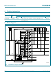
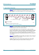
The slave address of the PCA9646 is shown in Figure 4. The address pins (A2, A1, A0)
must be driven to a HIGH or LOW level—they are not internally pulled to a default state.
The read/write bit must be set LOW to enable a write to the Control register, or HIGH to
read from the Control register.
7.8 Control register
The Control register of the PCA9646 is shown in Figure 5. Each of the four output
channels (SCn/SDn pairs) can be enabled independently, and the direction of the clock
signal can be reversed.
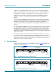
Fig 4. Slave address
002aaf368
1 1 1 0 A2 A1 A0 R/W
fixed externally
selectable
read = 1
write = 0
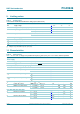
Fig 5. Control register
002aaf369
B7 X X X B3 B2 B1 B0
output channel
enable bits
MSB LSB
SCL direction
0: SCL → SC0 to SC3
1: SC0 to SC3 → SCL
SC0/SD0 enable
SC1/SD1 enable
SC2/SD2 enable
SC3/SD3 enable