
Datasheet

PCA9646 All information provided in this document is subject to legal disclaimers. © NXP B.V. 2011. All rights reserved.
Product data sheet Rev. 1 — 1 March 2011 3 of 22
NXP Semiconductors
PCA9646
Buffered 4-channel 2-wire bus switch
6. Pinning information
6.1 Pinning
6.2 Pin description
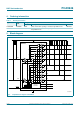
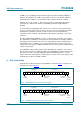
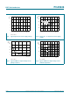
Fig 2. Pin configuration for SO16 Fig 3. Pin configuration for TSSOP16
PCA9646D
A0 V
DD
A1 SDA
RESET SCL
SD0 A2
SC0 SC3
SD1 SD3
SC1 SC2
V
SS
SD2
002aaf364
1
2
3
4
5
6
7
8
10
9
12
11
14
13
16
15
PCA9646PW
002aaf366
1
2
3
4
5
6
7
8
10
9
12
11
14
13
16
15
A0 V
DD
A1 SDA
RESET SCL
SD0 A2
SC0 SC3
SD1 SD3
SC1 SC2
V
SS
SD2
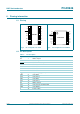
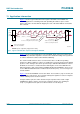
Table 2. Pin description
Symbol Pin Description
A0 1 address input 0
A1 2 address input 1
RESET
3 active LOW reset input
SD0 4 serial data 0
SC0 5 serial clock 0
SD1 6 serial data 1
SC1 7 serial clock 1
V
SS
8 negative supply (ground)
SD2 9 serial data 2
SC2 10 serial clock 2
SD3 11 serial data 3
SC3 12 serial clock 3
A2 13 address input 2
SCL 14 serial clock line (normally input)
SDA 15 serial data line
V
DD
16 positive supply