
Datasheet


NXP Semiconductors
PCA9646
Buffered 4-channel 2-wire bus switch
© NXP B.V. 2011. All rights reserved.
For more information, please visit: http://www.nxp.com
For sales office addresses, please send an email to: salesaddresses@nxp.com
Date of release: 1 March 2011
Document identifier: PCA9646
Please be aware that important notices concerning this document and the product(s)
described herein, have been included in section ‘Legal information’.
20. Contents
1 General description. . . . . . . . . . . . . . . . . . . . . . 1
2 Features and benefits . . . . . . . . . . . . . . . . . . . . 1
3 Applications . . . . . . . . . . . . . . . . . . . . . . . . . . . . 1
4 Ordering information. . . . . . . . . . . . . . . . . . . . . 2
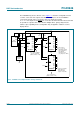
5 Block diagram . . . . . . . . . . . . . . . . . . . . . . . . . . 2
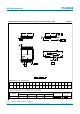
6 Pinning information. . . . . . . . . . . . . . . . . . . . . . 3
6.1 Pinning . . . . . . . . . . . . . . . . . . . . . . . . . . . . . . . 3
6.2 Pin description . . . . . . . . . . . . . . . . . . . . . . . . . 3
7 Functional description . . . . . . . . . . . . . . . . . . . 4
7.1 V
DD
, V
SS
— DC supply pins . . . . . . . . . . . . . . . 4
7.2 SCL — clock signal input . . . . . . . . . . . . . . . . . 4
7.3 SC0, SC1, SC2, SC3 — clock signal outputs. . 4
7.4 SDA, SD0, SD1, SD2, SD3 — data signal
inputs/outputs . . . . . . . . . . . . . . . . . . . . . . . . . . 4
7.5 RESET
— reset IC to default state. . . . . . . . . . 5
7.6 Power-On Reset (POR) . . . . . . . . . . . . . . . . . . 5
7.7 A0, A1, A2 — address lines . . . . . . . . . . . . . . . 5
7.8 Control register. . . . . . . . . . . . . . . . . . . . . . . . . 5
8 Bus transaction . . . . . . . . . . . . . . . . . . . . . . . . . 6
9 Limiting values. . . . . . . . . . . . . . . . . . . . . . . . . . 7
10 Characteristics. . . . . . . . . . . . . . . . . . . . . . . . . . 7
11 Application information. . . . . . . . . . . . . . . . . . 10
12 Package outline . . . . . . . . . . . . . . . . . . . . . . . . 14
13 Handling information. . . . . . . . . . . . . . . . . . . . 16
14 Soldering of SMD packages . . . . . . . . . . . . . . 16
14.1 Introduction to soldering . . . . . . . . . . . . . . . . . 16
14.2 Wave and reflow soldering . . . . . . . . . . . . . . . 16
14.3 Wave soldering. . . . . . . . . . . . . . . . . . . . . . . . 17
14.4 Reflow soldering. . . . . . . . . . . . . . . . . . . . . . . 17
15 Abbreviations. . . . . . . . . . . . . . . . . . . . . . . . . . 18
16 References . . . . . . . . . . . . . . . . . . . . . . . . . . . . 18
17 Revision history. . . . . . . . . . . . . . . . . . . . . . . . 19
18 Legal information. . . . . . . . . . . . . . . . . . . . . . . 20
18.1 Data sheet status . . . . . . . . . . . . . . . . . . . . . . 20
18.2 Definitions. . . . . . . . . . . . . . . . . . . . . . . . . . . . 20
18.3 Disclaimers. . . . . . . . . . . . . . . . . . . . . . . . . . . 20
18.4 Trademarks. . . . . . . . . . . . . . . . . . . . . . . . . . . 21
19 Contact information. . . . . . . . . . . . . . . . . . . . . 21
20 Contents . . . . . . . . . . . . . . . . . . . . . . . . . . . . . . 22