
Datasheet

PCA9646 All information provided in this document is subject to legal disclaimers. © NXP B.V. 2011. All rights reserved.
Product data sheet Rev. 1 — 1 March 2011 2 of 22
NXP Semiconductors
PCA9646
Buffered 4-channel 2-wire bus switch
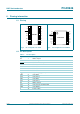
4. Ordering information
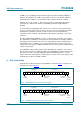
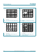
5. Block diagram
Table 1. Ordering information
Type number Topside
mark
Package
Name Description Version
PCA9646D PCA9646 SO16 plastic small outline package; 16 leads; body width 3.9 mm SOT109-1
PCA9646PW PCA9646 TSSOP16 plastic thin shrink small outline package; 16 leads;
body width 4.4 mm
SOT403-1
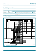
Fig 1. Simplified block diagram of PCA9646
R4
002aaf367
I
2
C-BUS
CONTROL
5
7
10
12
4
6
9
11
SC0
SC1
SC2
SC3
SD0
SD1
SD2
SD3
R3 R5 R6 R7 R8 R9 R10
V
DD
16
FILTER
1 A0
2 A1
13 A2
14
15
3
SCL
SDA
RESET
R2R1
2.7 V to 5.5 V
PCA9646
V
SS
8