
Datasheet


PCA9646 All information provided in this document is subject to legal disclaimers. © NXP B.V. 2011. All rights reserved.
Product data sheet Rev. 1 — 1 March 2011 13 of 22
NXP Semiconductors
PCA9646
Buffered 4-channel 2-wire bus switch
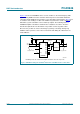
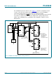
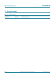
The PCA9646 may also be driven in series. Figure 17 shows this configuration. In this
scenario, each of the four outputs of the first device (U2) has six more PCA9646’s
connected to it. Each of those six devices has four outputs, thus giving
4 7 4 = 112 outputs. If the RESET
pin on U2 was also driven from the master, it would
be possible to reproduce this entire structure multiple times, giving a truly massive
address space capability. Such a configuration may be applied to situations such as
display drivers.
Fig 17. PCA9646 series implementation for large I/O fan-out
002aaf378
SCL
SCL
SDA
PCA9646
V
DD
SC0
SC1
U2
RESET
5 V
R1
180 Ω
R2
180 Ω
A[2:0]
SD0
SD1
SC2
SC3
SD2
SD3
3
BUS
MASTER
U1
V
DD
SCL
SDA
000b
up to seven PCA9646s
on each output pair
(address: 001b to 111b)
structure in
dashed box
repeated
etc.
R4
180 Ω
R3
180 Ω
SCL
SDA
PCA9646
V
DD
SC0
SC1
U3
RESET
SD0
SD1
SC2
SC3
SD2
SD3
A[2:0]
3
001b
total output of
4 × 7 × 4 = 112
individually enabled
fully isolated buses,
each with full
capacitance load
(e.g., 400 pF at 1 MHz)
5 V
SCL
SDA
PCA9646
V
DD
SC0
SC1
U4
RESET
SD0
SD1
SC2
SC3
SD2
SD3
A[2:0]
3
010b
connect, for example,
8 LED driver ICs,
each with 8 LED
outputs = 7168 LEDs
up to seven devices
(address: 001b to 111b)