
Datasheet

PCA9646 All information provided in this document is subject to legal disclaimers. © NXP B.V. 2011. All rights reserved.
Product data sheet Rev. 1 — 1 March 2011 10 of 22
NXP Semiconductors
PCA9646
Buffered 4-channel 2-wire bus switch
11. Application information
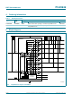
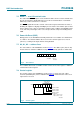
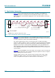
Figure 13 shows a typical data transfer through the PCA9646. The PCA9646 has
excellent application to extending loads and expanding the address space of slave
devices. Rise times are determined simply by the side of the buffer with the slowest RC
time constant.
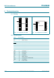
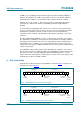
Figure 14 shows a typical application for the PCA9646. Each channel can support up to
the maximum permissible capacitance load, thus the maximum loading of the system can
be 5 times that which could be achieved without buffering.
The channel enable function can be used to interface buses of different operating
frequencies. When certain bus sections are enabled, the system frequency may be limited
by a bus section having a slave device specified only to 100 kHz. When that bus section is
disabled, the slow slave is isolated and the remaining bus can be run at 400 kHz. The
timing performance and current sinking capability will allow the PCA9646 to run in excess
of the 1 MHz maximum limit of the I
2
C-bus Fast-mode Plus (Fm+), or to run a huge 4 nF
load at 100 kHz.
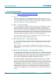
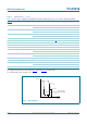
Figure 15
shows the PCA9646 used as a line driver. Four such lines (only one shown) can
be run from the same device. The receiving end may then again be used as a 4-way bus
switch, radiating out into another four lines.
Using the address pins, this entire structure may be repeated. Thus a total of eight
PCA9646 ‘line drivers’ may be connected to a single bus master (U1), allowing for
32 (8 4) long distance bus pairs to be driven from the one I
2
C-bus port.
Remark: Input to output delay exaggerated for clarity.
Fig 13. Typical communication sequence through the PCA9646
002aaf374
S
START
sequence
SCL
(clock)
SDA
(data)
A0
(master)
A1
(master)
A2
(master)
master side of PCA9646
slave side of PCA9646
purpose of bit (address bit 5)
device asserting data line (master/slave)
A3
(master)
A4
(master)
A5
(master)
A6
(master)
SDA direction
'hand over' pulses upon change
of device asserting the data line
W
(master)
ACK
(slave)
P
STOP
sequence