
Datasheet


PCA9539A All information provided in this document is subject to legal disclaimers. © NXP B.V. 2013. All rights reserved.
Product data sheet Rev. 2 — 12 August 2013 8 of 39
NXP Semiconductors
PCA9539A
Low voltage 16-bit I
2
C-bus I/O port with interrupt and reset
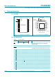
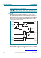
6.3 I/O port
When an I/O is configured as an input, FETs Q1 and Q2 are off, which creates a
high-impedance input. The input voltage may be raised above V
DD
to a maximum of 5.5 V.
If the I/O is configured as an output, Q1 or Q2 is enabled, depending on the state of the
Output port register. In this case, there are low-impedance paths between the I/O pin and
either V
DD
or V
SS
. The external voltage applied to this I/O pin should not exceed the
recommended levels for proper operation.
6.4 Power-on reset
When power (from 0 V) is applied to V
DD
, an internal power-on reset holds the PCA9539A
in a reset condition until V
DD
has reached V
POR
. At that time, the reset condition is
released and the PCA9539A registers and I
2
C-bus/SMBus state machine initializes to
their default states. After that, V
DD
must be lowered to below V
PORF
and back up to the
operating voltage for a power-reset cycle. See Section 8.2 “
Power-on reset requirements”.
Table 12. Configuration port 1 register (address 07h)
Bit 7 6 5 4 3 2 1 0
Symbol C1.7 C1.6 C1.5 C1.4 C1.3 C1.2 C1.1 C1.0
Default 11111111
At power-on reset, all registers return to default values.
Fig 6. Simplified schematic of the I/Os (P0_0 to P0_7, P1_0 to P1_7)
V
DD
P0_0 to P0_7
P1_0 to P1_7
output port
register data
configuration
register
DQ
CK Q
data from
shift register
write
configuration
pulse
output port
register
DQ
CK
write pulse
polarity
inversion
register
DQ
CK
data from
shift register
write polarity
pulse
input port
register
DQ
CK
read pulse
input port
register data
polarity
inversion
register data
002aah246
FF
data from
shift register
FF
FF
FF
Q1
Q2
V
SS
to INT
ESD
protection
diode