
Datasheet


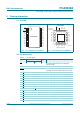

PCA9539A All information provided in this document is subject to legal disclaimers. © NXP B.V. 2013. All rights reserved.
Product data sheet Rev. 2 — 12 August 2013 7 of 39
NXP Semiconductors
PCA9539A
Low voltage 16-bit I
2
C-bus I/O port with interrupt and reset
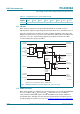
6.2.3 Output port register pair (02h, 03h)
The Output port registers (registers 2 and 3) show the outgoing logic levels of the pins
defined as outputs by the Configuration register. Bit values in these registers have no
effect on pins defined as inputs. In turn, reads from these registers reflect the value that
was written to these registers, not the actual pin value. A register pair write is described in
Section 7.1
and a register pair read is described in Section 7.2.
6.2.4 Polarity inversion register pair (04h, 05h)
The Polarity inversion registers (registers 4 and 5) allow polarity inversion of pins defined
as inputs by the Configuration register. If a bit in these registers is set (written with ‘1’), the
corresponding port pin’s polarity is inverted in the Input register. If a bit in this register is
cleared (written with a ‘0’), the corresponding port pin’s polarity is retained. A register pair
write is described in Section 7.1
and a register pair read is described in Section 7.2.
6.2.5 Configuration register pair (06h, 07h)
The Configuration registers (registers 6 and 7) configure the direction of the I/O pins. If a
bit in these registers is set to 1, the corresponding port pin is enabled as a
high-impedance input. If a bit in these registers is cleared to 0, the corresponding port pin
is enabled as an output. A register pair write is described in Section 7.1
and a register pair
read is described in Section 7.2
.
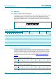
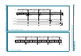
Table 7. Output port 0 register (address 02h)
Bit 7 6 5 4 3 2 1 0
Symbol O0.7 O0.6 O0.5 O0.4 O0.3 O0.2 O0.1 O0.0
Default 11111111
Table 8. Output port 1 register (address 03h)
Bit 7 6 5 4 3 2 1 0
Symbol O1.7 O1.6 O1.5 O1.4 O1.3 O1.2 O1.1 O1.0
Default 11111111
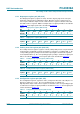
Table 9. Polarity inversion port 0 register (address 04h)
Bit 7 6 5 4 3 2 1 0
Symbol N0.7 N0.6 N0.5 N0.4 N0.3 N0.2 N0.1 N0.0
Default 00000000
Table 10. Polarity inversion port 1 register (address 05h)
Bit 7 6 5 4 3 2 1 0
Symbol N1.7 N1.6 N1.5 N1.4 N1.3 N1.2 N1.1 N1.0
Default 00000000
Table 11. Configuration port 0 register (address 06h)
Bit 7 6 5 4 3 2 1 0
Symbol C0.7 C0.6 C0.5 C0.4 C0.3 C0.2 C0.1 C0.0
Default 11111111