
Datasheet


PCA9539A All information provided in this document is subject to legal disclaimers. © NXP B.V. 2013. All rights reserved.
Product data sheet Rev. 2 — 12 August 2013 5 of 39
NXP Semiconductors
PCA9539A
Low voltage 16-bit I
2
C-bus I/O port with interrupt and reset
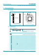
[1] HWQFN24 package die supply ground is connected to both V
SS
pin and exposed center pad. V
SS
pin must
be connected to supply ground for proper device operation. For enhanced thermal, electrical, and board
level performance, the exposed pad needs to be soldered to the board using a corresponding thermal pad
on the board and for proper heat conduction through the board, thermal vias need to be incorporated in the
PCB in the thermal pad region.
[2] Pins P0_0 to P0_7 correspond to bits P0.0 to P0.7. At power-up, all I/O are configured as high-impedance
inputs.
[3] Pins P1_0 to P1_7 correspond to bits P1.0 to P1.7. At power-up, all I/O are configured as high-impedance
inputs.
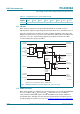
6. Functional description
Refer to Figure 1 “Block diagram of PCA9539A”.
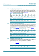
6.1 Device address
A1 and A0 are the hardware address package pins and are held to either HIGH (logic 1)
or LOW (logic 0) to assign one of the four possible slave addresses. The last bit of the
slave address (R/W
) defines the operation (read or write) to be performed. A HIGH
(logic 1) selects a read operation, while a LOW (logic 0) selects a write operation.
P1_6
[3]
19 16 I/O Port 1 input/output 6.
P1_7
[3]
20 17 I/O Port 1 input/output 7.
A0 21 18 I Address input 0. Connect directly to V
DD
or V
SS
.
SCL 22 19 I Serial clock bus. Connect to V
DD
through a
pull-up resistor.
SDA 23 20 I/O Serial data bus. Connect to V
DD
through a
pull-up resistor.
V
DD
24 21 power Supply voltage.
Table 3. Pin description …continued
Symbol Pin Type Description
TSSOP24 HWQFN24
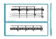
Fig 4. PCA9539A device address
R/W
002aah062
1 1 1 0 1 A1 A0
hardware
selectable
slave address
fixed