
Datasheet


PCA9539A All information provided in this document is subject to legal disclaimers. © NXP B.V. 2013. All rights reserved.
Product data sheet Rev. 2 — 12 August 2013 3 of 39
NXP Semiconductors
PCA9539A
Low voltage 16-bit I
2
C-bus I/O port with interrupt and reset
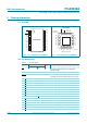
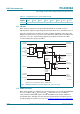
4. Block diagram
Remark: All I/Os are set to inputs at reset.
Fig 1. Block diagram of PCA9539A
PCA9539A
POWER-ON
RESET
002aag162
I
2
C-BUS/SMBus
CONTROL
INPUT
FILTER
SCL
SDA
V
DD
INPUT/
OUTPUT
PORTS
P0_0
V
SS
8-bit
write pulse
read pulse
P0_2
P0_1
P0_3
P0_4
P0_5
P0_6
P0_7
INPUT/
OUTPUT
PORTS
P1_0
8-bit
write pulse
read pulse
P1_2
P1_1
P1_3
P1_4
P1_5
P1_6
P1_7
A1
A0
RESET
LP
FILTER
V
DD
INT