
Datasheet


NXP Semiconductors
PCA9535A
Low-voltage 16-bit I
2
C-bus I/O port with interrupt
© NXP B.V. 2012. All rights reserved.
For more information, please visit: http://www.nxp.com
For sales office addresses, please send an email to: salesaddresses@nxp.com
Date of release: 11 September 2012
Document identifier: PCA9535A
Please be aware that important notices concerning this document and the product(s)
described herein, have been included in section ‘Legal information’.
23. Contents
1 General description . . . . . . . . . . . . . . . . . . . . . . 1
2 Features and benefits . . . . . . . . . . . . . . . . . . . . 1
3 Ordering information. . . . . . . . . . . . . . . . . . . . . 2
3.1 Ordering options. . . . . . . . . . . . . . . . . . . . . . . . 2
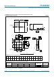
4 Block diagram . . . . . . . . . . . . . . . . . . . . . . . . . . 3
5 Pinning information. . . . . . . . . . . . . . . . . . . . . . 3
5.1 Pinning . . . . . . . . . . . . . . . . . . . . . . . . . . . . . . . 3
5.2 Pin description . . . . . . . . . . . . . . . . . . . . . . . . . 4
6 Functional description . . . . . . . . . . . . . . . . . . . 5
6.1 Device address. . . . . . . . . . . . . . . . . . . . . . . . . 5
6.2 Registers . . . . . . . . . . . . . . . . . . . . . . . . . . . . . 5
6.2.1 Pointer register and command byte . . . . . . . . . 5
6.2.2 Input port register pair (00h, 01h). . . . . . . . . . . 6
6.2.3 Output port register pair (02h, 03h) . . . . . . . . . 6
6.2.4 Polarity inversion register pair (04h, 05h). . . . . 7
6.2.5 Configuration register pair (06h, 07h). . . . . . . . 7
6.3 I/O port . . . . . . . . . . . . . . . . . . . . . . . . . . . . . . . 8
6.4 Power-on reset . . . . . . . . . . . . . . . . . . . . . . . . . 9
6.5 Interrupt output . . . . . . . . . . . . . . . . . . . . . . . . . 9
7 Bus transactions . . . . . . . . . . . . . . . . . . . . . . . . 9
7.1 Writing to the port registers. . . . . . . . . . . . . . . . 9
7.2 Reading the port registers . . . . . . . . . . . . . . . 11
8 Application design-in information . . . . . . . . . 14
8.1 Minimizing I
DD
when the I/Os are used to
control LEDs. . . . . . . . . . . . . . . . . . . . . . . . . . 14
8.2 Power-on reset requirements . . . . . . . . . . . . . 15
9 Limiting values. . . . . . . . . . . . . . . . . . . . . . . . . 17
10 Recommended operating conditions. . . . . . . 17
11 Thermal characteristics . . . . . . . . . . . . . . . . . 17
12 Static characteristics. . . . . . . . . . . . . . . . . . . . 18
12.1 Typical characteristics . . . . . . . . . . . . . . . . . . 20
13 Dynamic characteristics . . . . . . . . . . . . . . . . . 24
14 Parameter measurement information . . . . . . 25
15 Package outline . . . . . . . . . . . . . . . . . . . . . . . . 28
16 Handling information. . . . . . . . . . . . . . . . . . . . 30
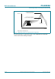
17 Soldering of SMD packages . . . . . . . . . . . . . . 30
17.1 Introduction to soldering . . . . . . . . . . . . . . . . . 30
17.2 Wave and reflow soldering . . . . . . . . . . . . . . . 30
17.3 Wave soldering. . . . . . . . . . . . . . . . . . . . . . . . 30
17.4 Reflow soldering . . . . . . . . . . . . . . . . . . . . . . . 31
18 Soldering: PCB footprints. . . . . . . . . . . . . . . . 33
19 Abbreviations. . . . . . . . . . . . . . . . . . . . . . . . . . 35
20 Revision history. . . . . . . . . . . . . . . . . . . . . . . . 35
21 Legal information. . . . . . . . . . . . . . . . . . . . . . . 36
21.1 Data sheet status . . . . . . . . . . . . . . . . . . . . . . 36
21.2 Definitions . . . . . . . . . . . . . . . . . . . . . . . . . . . 36
21.3 Disclaimers . . . . . . . . . . . . . . . . . . . . . . . . . . 36
21.4 Trademarks . . . . . . . . . . . . . . . . . . . . . . . . . . 37
22 Contact information . . . . . . . . . . . . . . . . . . . . 37
23 Contents. . . . . . . . . . . . . . . . . . . . . . . . . . . . . . 38