
Datasheet


PCA9535A All information provided in this document is subject to legal disclaimers. © NXP B.V. 2012. All rights reserved.
Product data sheet Rev. 1 — 11 September 2012 27 of 38
NXP Semiconductors
PCA9535A
Low-voltage 16-bit I
2
C-bus I/O port with interrupt
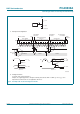
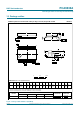
a. P port load configuration
b. Write mode (R/W =0)
c. Read mode (R/W
=1)
C
L
includes probe and jig capacitance.
t
v(Q)
is measured from 0.7 V
DD
on SCL to 50 % I/O (Pn) output.
All inputs are supplied by generators having the following characteristics: PRR 10 MHz; Z
o
=50; t
r
/t
f
30 ns.
The outputs are measured one at a time, with one transition per measurement.
All parameters and waveforms are not applicable to all devices.
Fig 28. P port load circuit and voltage waveforms
002aag805
DUT
C
L
= 50 pF
500 Ω
Pn
2 × V
DD
500 Ω
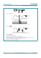
002aag806
SCL
SDA
P0 A
t
v(Q)
0.3 × V
DD
0.7 × V
DD
P7
last stable bit
unstable
data
Pn
002aag807
SCL
Pn
P0 A
t
h(D)
0.3 × V
DD
0.7 × V
DD
P7
t
su(D)