
Datasheet

PCA9518A_3 © NXP B.V. 2008. All rights reserved.
Product data sheet Rev. 03 — 3 December 2008 8 of 23
NXP Semiconductors
PCA9518A
Expandable 5-channel I
2
C-bus hub
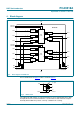
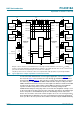
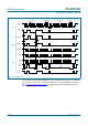
the acknowledge and then returns to the PCA9518A level creating a foot before it
completes the LOW-to-HIGH transition. SDA lines other than the one with the master and
the one with the slave have a uniform LOW level driven by the PCA9518A repeater.
The other four waveforms are the expansion bus signals and are included primarily for
timing reference points. All timing on the expansion bus is with respect to 0.5V
DD
.
EXPSDA1 is the expansion bus that is driven LOW whenever any SDA pin falls below
0.3V
DD
. EXPSDA2 is the expansion bus that is driven LOW whenever any pin is ≤0.4 V.
EXPSCL1 is the expansion bus that is driven LOW whenever any SCL pin falls below
0.3V
DD
. EXPSCL2 is the expansion bus that is driven LOW whenever any SCL pin is
≤0.4 V. The EXPSDA2 returns HIGH after the SDA pin that was the last one being held
below 0.4 V by an external driver starts to rise. The last SDA to rise above 0.4 V is held
down by the PCA9518A to ~0.5 V until after the delay of the circuit which determines that
it was the last to rise, then it is allowed to rise above the ~0.5 V level driven by the
PCA9518A. Considering the bus 0 SDA to be the last one to go above 0.4 V, then the
EXPSDA1 returns to HIGH after the EXPSDA2 is HIGH and either the bus 0 SDA rise time
is 1 µs or, when the bus 0 SDA reaches 0.7V
DD
, whichever occurs first. After both
EXPSDA2 and EXPSDA1 are HIGH the rest of the SDA lines are allowed to rise. The
same description applies for the EXPSCL1, EXPSCL2, and SCL pins.