
Datasheet

PCA9518A_3 © NXP B.V. 2008. All rights reserved.
Product data sheet Rev. 03 — 3 December 2008 3 of 23
NXP Semiconductors
PCA9518A
Expandable 5-channel I
2
C-bus hub
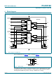
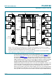
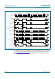
4. Block diagram
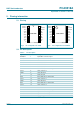
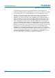
A more detailed view of Figure 1 buffer is shown in Figure 2.
The output pull-down voltage of each internal buffer is set for approximately 0.5 V, while
the input threshold of each internal buffer is set about 0.07 V lower, when the output is
internally driven LOW. This prevents a lock-up condition from occurring.
Fig 1. Block diagram of PCA9518A
PCA9518A
002aac530
EXPSCL1
V
DD
EXPSCL2
EXPSDA2
SCL0
EXPSDA1
SDA0
EN4
SCL1
SDA4
SDA1
SCL4
EN1
EN3
SCL2
SDA3
SDA2
SCL3
V
SS
BUFFER
BUFFER
BUFFER
HUB
LOGIC
BUFFER
BUFFER
BUFFER
BUFFER
BUFFER
HUB
LOGIC
BUFFER
BUFFER
EN2
Fig 2. Buffer detail
002aac531
to output
in
inc
data
enable