
Datasheet

PCA9515A All information provided in this document is subject to legal disclaimers. © NXP B.V. 2012. All rights reserved.
Product data sheet Rev. 5 — 23 March 2012 6 of 20
NXP Semiconductors
PCA9515A
I
2
C-bus repeater
8. Limiting values
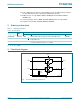
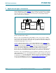
Fig 6. Bus 0 waveform
9
th
clock pulse
V
OL
of master
V
OL
of PCA9515A
002aad740
SCL
SDA
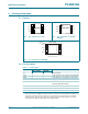
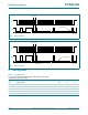
Fig 7. Bus 1 waveform
9
th
clock pulse
V
OL
of slave
V
OL
of PCA9515A
002aad741
SCL
SDA
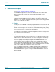
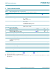
Table 3. Limiting values
In accordance with the Absolute Maximum Rating System (IEC 60134).
Voltages with respect to pin GND.
Symbol Parameter Conditions Min Max Unit
V
CC
supply voltage 0.5 +7 V
V
I2C-bus
I
2
C-bus voltage SCL or SDA 0.5 +7 V
I
I/O
input/output current DC; any pin - 50 mA
P
tot
total power dissipation - 100 mW
T
stg
storage temperature 55 +125 C
T
amb
ambient temperature operating in free air 40 +85 C