
Datasheet

PCA9515A All information provided in this document is subject to legal disclaimers. © NXP B.V. 2012. All rights reserved.
Product data sheet Rev. 5 — 23 March 2012 5 of 20
NXP Semiconductors
PCA9515A
I
2
C-bus repeater
7. Application design-in information
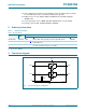
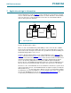
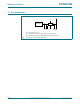
A typical application is shown in Figure 5. In this example, the system master is running
on a 3.3 V I
2
C-bus while the slave is connected to a 5 V bus. Both buses run at 100 kHz
unless the slave bus is isolated and then the master bus can run at 400 kHz. Master
devices can be placed on either bus.
The PCA9515A is 5 V tolerant, so it does not require any additional circuitry to translate
between the different bus voltages.
When one side of the PCA9515A is pulled LOW by a device on the I
2
C-bus, a CMOS
hysteresis type input detects the falling edge and causes the internal driver on the other
side to turn on, thus causing the other side to also go LOW. The side driven LOW by the
PCA9515A will typically be at V
OL
=0.5V.
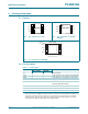
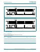
In order to illustrate what would be seen in a typical application, refer to Figure 6
and
Figure 7
. If the bus master in Figure 5 were to write to the slave through the PCA9515A,
we would see the waveform shown in Figure 6
on bus 0. This looks like a normal I
2
C-bus
transmission until the falling edge of the eighth clock pulse. At that point, the master
releases the data line (SDA) while the slave pulls it LOW through the PCA9515A.
Because the V
OL
of the PCA9515A is typically round 0.5 V, a step in the SDA will be seen.
After the master has transmitted the ninth clock pulse, the slave releases the data line.
On the bus 1 side of the PCA9515A, the clock and data lines would have a positive offset
from ground equal to the V
OL
of the PCA9515A. After the eighth clock pulse the data line
will be pulled to the V
OL
of the slave device, which is very close to ground in this example.
It is important to note that any arbitration or clock stretching events on bus 1 require that
the V
OL
of the PCA9515A (see V
OL
V
ILc
in Section 9 “Static characteristics”) to be
recognized by the PCA9515A and then transmitted to bus 0.
Fig 5. Typical application
002aad739
V
CC
PCA9515A
SDA0 SDA1
SCL0 SCL1
EN
10 kΩ
10 kΩ
SDA
SCL
BUS
MASTER
400 kHz
SLAVE
100 kHz
SDA
SCL
bus 0 bus 1
5 V
3.3 V
10 kΩ
10 kΩ