
Datasheet

PCA9515A All information provided in this document is subject to legal disclaimers. © NXP B.V. 2012. All rights reserved.
Product data sheet Rev. 5 — 23 March 2012 3 of 20
NXP Semiconductors
PCA9515A
I
2
C-bus repeater
5. Pinning information
5.1 Pinning
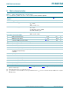
5.2 Pin description
[1] HWSON8 package die supply ground is connected to both GND pin and exposed center pad. GND pin
must be connected to supply ground for proper device operation. For enhanced thermal, electrical, and
board level performance, the exposed pad needs to be soldered to the board using a corresponding
thermal pad on the board and for proper head conduction through the board, thermal vias need to be
incorporated in the printed-circuit board in the thermal pad region.
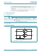
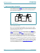
Fig 2. Pin configuration for SO8 Fig 3. Pin configuration for TSSOP8
(MSOP8)
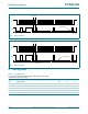
Fig 4. Pin configuration for HWSON8
n.c. V
CC
SCL0 SCL1
SDA0
SDA1
GND EN
002aad736
1
2
3
4
6
5
8
7
PCA9515AD
PCA9515ADP
n.c. V
CC
SCL0 SCL1
SDA0 SDA1
GND EN
002aad737
1
2
3
4
6
5
8
7
SDA0
GND
EN
SDA1
SCL0
n.c.
V
CC
SCL1
002aag783
terminal 1
index area
1
PCA9515ATP
Transparent top view
2
3
4
8
7
6
5
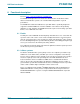
Table 2. Pin description
Symbol Pin Description
SO8, TSSOP8 HWSON8
n.c. 1 7 not connected
SCL0 2 8 serial clock bus 0; open-drain 5 V tolerant I/O
SDA0 3 1 serial data bus 0; open-drain 5 V tolerant I/O
GND 4 2
[1]
supply ground (0 V)
EN 5 3 active HIGH repeater enable input
(internal pull-up with 100 k)
SDA1 6 4 serial data bus 1; open-drain 5 V tolerant I/O
SCL1 7 5 serial clock bus 1; open-drain 5 V tolerant I/O
V
CC
8 6 supply voltage