
Datasheet


PCA9501_4 © NXP B.V. 2009. All rights reserved.
Product data sheet Rev. 04 — 10 February 2009 8 of 28
NXP Semiconductors
PCA9501
8-bit I
2
C-bus and SMBus I/O port with interrupt, 2-kbit EEPROM
7.4 Memory operations
7.4.1 Write operations
Write operations require an additional address field to indicate the memory address
location to be written. The address field is eight bits long providing access to any one of
the 256 words of memory. There are two types of write operations, ‘byte write’ and ‘page
write’.
Write operation is possible when the Write Control pin (WC) is put at a LOW logic level (0).
When this control signal is set at 1, write operation is not possible and data in the memory
is protected.
‘Byte write’ and ‘page write’ explained below assume that WC is set to 0.
7.4.1.1 Byte write
To perform a byte write, the START condition is followed by the memory slave address and
the R/W bit set to 0. The PCA9501 will respond with an acknowledge and then consider
the next eight bits sent as the word address and the eight bits after the word address as
the data. The PCA9501 will issue an acknowledge after the receipt of both the word
address and the data. To terminate the data transfer the master issues the STOP
condition, initiating the internal write cycle to the non-volatile memory. Only write and read
operations to the quasi-bidirectional I/Os are allowed during the internal write cycle.
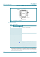
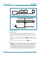
Fig 10. Application of multiple PCA9501s with interrupt
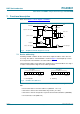
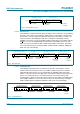
Fig 11. Interrupt generated by a change of input to IO5
002aad293
V
DD
MICROCONTROLLER
INT
PCA9501
INT
PCA9501
INT
device 1 device 2
PCA9501
INT
device 16
1 AS
slave address (I/O expander)
START condition R/W
acknowledge
from slave
002aad294
1
data from port
1
12345678SCL 9
SDA
data into IO5
INT
A5 A4 A3 A2 A1 A00
IO5
P
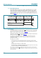
STOP
condition
t
v(INT)
t
rst(INT)