
Datasheet


PCA9501_4 © NXP B.V. 2009. All rights reserved.
Product data sheet Rev. 04 — 10 February 2009 6 of 28
NXP Semiconductors
PCA9501
8-bit I
2
C-bus and SMBus I/O port with interrupt, 2-kbit EEPROM
7.2 Control register
The PCA9501 contains a single 8-bit register called the Control register, which can be
written and read via the I
2
C-bus. This register is sent after a successful acknowledgment
of the slave address.
It contains the I/O operation information.
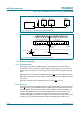
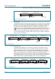
7.3 I/O operations
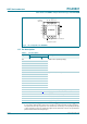
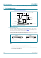
(Refer also to Figure 5.)
Each of the PCA9501's eight I/Os can be independently used as an input or output.
Output data is transmitted to the port by the I/O Write mode (see Figure 7). Input I/O data
is transferred from the port to the microcontroller by the Read mode (see Figure 8).
Fig 7. I/O Write mode (output)
0 AS
slave address (I/O expander)
START condition R/W acknowledge
from slave
002aad290
DATA 1
data to port
A
acknowledge
from slave
12345678SCL 9
SDA DATA 2 A
write to port
data out from port
t
v(Q)
acknowledge
from slave
DATA 2 VALID
data to port
A5 A4 A3 A2 A1 A00
DATA 1 VALID
t
v(Q)
Fig 8. I/O Read mode (input)
A5 A4 A3 A2 A1 A0 1 AS0
slave address (I/O expander)
START condition R/W
acknowledge
from slave
002aad291
data from port
A
acknowledge
from master
SDA 1
no acknowledge
from master
read from
port
data into
port
data from port
DATA 1
DATA 4
INT
DATA 4
DATA 2
DATA 3
P
STOP
condition
t
v(INT)
t
rst(INT)
t
h(D)
t
su(D)
12345678SCL 9
DATA 1