
Datasheet


PCA9501_4 © NXP B.V. 2009. All rights reserved.
Product data sheet Rev. 04 — 10 February 2009 4 of 28
NXP Semiconductors
PCA9501
8-bit I
2
C-bus and SMBus I/O port with interrupt, 2-kbit EEPROM
6.2 Pin description
[1] HVQFN20 package die supply ground is connected to both V
SS
pin and exposed center pad. V
SS
pin must
be connected to supply ground for proper device operation. For enhanced thermal, electrical, and board
level performance, the exposed pad needs to be soldered to the board using a corresponding thermal pad
on the board and for proper heat conduction through the board, thermal vias need to be incorporated in the
printed-circuit board in the thermal pad region.
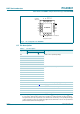
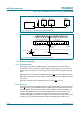
Fig 4. Pin configuration for HVQFN20
002aab999
PCA9501BS
Transparent top view
IO4
IO2
IO3
IO5
IO1 IO6
IO0 IO7
A2 WC
INT
A5
V
SS
A4
A3
A1
A0
V
DD
SDA
SCL
5 11
4 12
3 13
2 14
1 15
6
7
8
9
10
20
19
18
17
16
terminal 1
index area
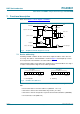
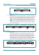
Table 3. Pin description
Symbol Pin Description
SO20, TSSOP20 HVQFN20
A0 1 19 address lines (internal pull-up)
A1 2 20
A2 3 1
A3 12 10
A4 11 9
A5 9 7
IO0 4 2 quasi-bidirectional I/O pins
IO1 5 3
IO2 6 4
IO3 7 5
IO4 13 11
IO5 14 12
IO6 15 13
IO7 16 14
INT 8 6 active LOW interrupt output (open-drain)
V
SS
10 8
[1]
supply ground
WC 17 15 active LOW write control pin
SCL 18 16 I
2
C-bus serial clock
SDA 19 17 I
2
C-bus serial data
V
DD
20 18 supply voltage