
Datasheet


PCA9501_4 © NXP B.V. 2009. All rights reserved.
Product data sheet Rev. 04 — 10 February 2009 14 of 28
NXP Semiconductors
PCA9501
8-bit I
2
C-bus and SMBus I/O port with interrupt, 2-kbit EEPROM
10. Limiting values
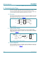
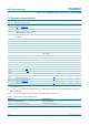
GPIO device address configured as 0110 000x for this example.
EEPROM device address configured as 1110 000x for this example.
IO0, IO2, IO3 configured as outputs.
IO1, IO4, IO5 configured as inputs.
IO6, IO7 are not used and must be configured as outputs.
Fig 22. Typical application
PCA9501
IO0
IO1
SCL
SDA
V
DD
MASTER
CONTROLLER
SCL
SDA
10 kΩ
IO2
V
DD
A2
A1
A0
V
DD
INT
V
SS
INT
10 kΩ
(optional)
SUB-SYSTEM 1
(e.g., temp sensor)
IO3
INT
SUB-SYSTEM 2
(e.g., counter)
RESET
controlled
switch
(e.g., CBT device)
V
DD
A
B
enable
SUB-SYSTEM 3
(e.g., alarm system)
ALARM
IO4
IO5
V
SS
A3
IO6
IO7
2 kΩ
10 kΩ10 kΩ
A4
A5
002aac025
Table 4. Limiting values
In accordance with the Absolute Maximum Rating System (IEC 60134).
Symbol Parameter Conditions Min Max Unit
V
DD
supply voltage −0.5 +4.0 V
V
I
input voltage V
SS
− 0.5 5.5 V
I
I
input current −20 +20 mA
I
O
output current −25 +25 mA
I
DD
supply current −100 +100 mA
I
SS
ground supply current −100 +100 mA
P
tot
total power dissipation - 400 mW
P/out power dissipation per output - 100 mW
T
stg
storage temperature −65 +150 °C
T
amb
ambient temperature operating −40 +85 °C