
Single-Chip Microcontroller User Manual


UM10310_1 © NXP B.V. 2008. All rights reserved.
User manual Rev. 01 — 1 December 2008 7 of 139
NXP Semiconductors
UM10310
P89LPC9321 User manual
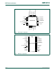
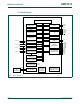
[1] Input/output for P1.0 to P1.4, P1.6, P1.7. Input for P1.5.
P2.5/SPICLK 16 I/O P2.5 — Port 2 bit 5.
I/O SPICLK — SPI clock. When configured as master, this pin is output; when
configured as slave, this pin is input.
P2.6/OCA 27 I/O P2.6 — Port 2 bit 6.
O OCA — Output Compare A.
P2.7/ICA 28 I/O P2.7 — Port 2 bit 7.
I ICA — Input Capture A.
P3.0 to P3.1 I/O Port 3: Port 3 is a 2-bit I/O port with a user-configurable output type. During reset
Port 3 latches are configured in the input only mode with the internal pull-up
disabled. The operation of Port 3 pins as inputs and outputs depends upon the
port configuration selected. Each port pin is configured independently. Refer to
Section 4.1 “
Port configurations” for details.
All pins have Schmitt triggered inputs.
Port 3 also provides various special functions as described below:
P3.0/XTAL2/
CLKOUT
9I/OP3.0 — Port 3 bit 0.
O XTAL2 — Output from the oscillator amplifier (when a crystal oscillator option is
selected via the flash configuration.
O CLKOUT — CPU clock divided by 2 when enabled via SFR bit (ENCLK -TRIM.6).
It can be used if the CPU clock is the internal RC oscillator, watchdog oscillator or
external clock input, except when XTAL1/XTAL2 are used to generate clock
source for the RTC/system timer.
P3.1/XTAL1 8 I/O P3.1 — Port 3 bit 1.
I XTAL1 — Input to the oscillator circuit and internal clock generator circuits (when
selected via the flash configuration). It can be a port pin if internal RC oscillator or
watchdog oscillator is used as the CPU clock source, and if XTAL1/XTAL2 are not
used to generate the clock for the RTC/system timer.
V
SS
7IGround: 0 V reference.
V
DD
21 I Power supply: This is the power supply voltage for normal operation as well as
Idle and Power-down modes.
Table 1. Pin description …continued
Symbol Pin Type Description