UM10310 P89LPC9321 User manual Rev.
UM10310 NXP Semiconductors P89LPC9321 User manual Revision history Rev Date Description 01 20081201 Initial version. Contact information For more information, please visit: http://www.nxp.com For sales office addresses, please send an email to: salesaddresses@nxp.com UM10310_1 User manual © NXP B.V. 2008. All rights reserved. Rev.
UM10310 NXP Semiconductors P89LPC9321 User manual 1. Introduction The P89LPC9321 is a single-chip microcontroller designed for applications demanding high-integration, low cost solutions over a wide range of performance requirements. The P89LPC9321 is based on a high performance processor architecture that executes instructions in two to four clocks, six times the rate of standard 80C51 devices.
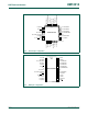
UM10310 NXP Semiconductors P2.0/ICB 1 26 P0.1/CIN2B/KBI1 P2.1/OCD 2 27 P2.6/OCA P0.0/CMP2/KBI0 3 28 P2.7/ICA P1.7/OCC 4 P89LPC9321 User manual P1.6/OCB 5 25 P0.2/CIN2A/KBI2 P1.5/RST 6 24 P0.3/CIN1B/KBI3 VSS 7 23 P0.4/CIN1A/KBI4 P3.1/XTAL1 8 P3.0/XTAL2/CLKOUT 9 22 P0.5/CMPREF/KBI5 P89LPC9321FA 21 VDD 20 P0.6/CMP1/KBI6 P1.4/INT1 10 19 P0.7/T1/KBI7 Fig 2. P1.0/TXD 18 P1.1/RXD 17 P2.5/SPICLK 16 P2.4/SS 15 P2.3/MISO 14 P2.2/MOSI 13 P1.2/T0/SCL 12 P1.
UM10310 NXP Semiconductors P89LPC9321 User manual 1.2 Pin description Table 1. Pin description Symbol Pin P0.0 to P0.7 Type Description I/O Port 0: Port 0 is an 8-bit I/O port with a user-configurable output type. During reset Port 0 latches are configured in the input only mode with the internal pull-up disabled. The operation of Port 0 pins as inputs and outputs depends upon the port configuration selected. Each port pin is configured independently. Refer to Section 4.
UM10310 NXP Semiconductors P89LPC9321 User manual Table 1. Pin description …continued Symbol Pin Type Description P1.0/TXD 18 I/O P1.0 — Port 1 bit 0. O TXD — Transmitter output for serial port. I/O P1.1 — Port 1 bit 1. I RXD — Receiver input for serial port. I/O P1.2 — Port 1 bit 2 (open-drain when used as output). I/O T0 — Timer/counter 0 external count input or overflow output (open-drain when used as output). I/O SCL — I2C-bus serial clock input/output. I/O P1.
UM10310 NXP Semiconductors P89LPC9321 User manual Table 1. Pin description …continued Symbol Pin Type Description P2.5/SPICLK 16 I/O P2.5 — Port 2 bit 5. I/O SPICLK — SPI clock. When configured as master, this pin is output; when configured as slave, this pin is input. I/O P2.6 — Port 2 bit 6. O OCA — Output Compare A. I/O P2.7 — Port 2 bit 7. P2.6/OCA P2.7/ICA 27 28 P3.0 to P3.1 I ICA — Input Capture A. I/O Port 3: Port 3 is a 2-bit I/O port with a user-configurable output type.
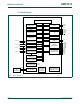
UM10310 NXP Semiconductors P89LPC9321 User manual 1.3 Functional diagram VDD KBI0 KBI1 KBI2 KBI3 KBI4 KBI5 KBI6 KBI7 CMP2 CIN2B CIN2A CIN1B CIN1A CMPREF CMP1 T1 CLKOUT XTAL2 VSS PORT 0 PORT 1 TXD RXD T0 INT0 INT1 RST OCB OCC PORT 2 ICB OCD MOSI MISO SS SPICLK OCA ICA P89LPC9321 PORT 3 XTAL1 SCL SDA 002aae103 Fig 4. Functional diagram UM10310_1 User manual © NXP B.V. 2008. All rights reserved. Rev.
UM10310 NXP Semiconductors P89LPC9321 User manual 1.
UM10310 NXP Semiconductors P89LPC9321 User manual 1.5 Special function registers Remark: SFR accesses are restricted in the following ways: • User must not attempt to access any SFR locations not defined. • Accesses to any defined SFR locations must be strictly for the functions for the SFRs. • SFR bits labeled ‘-’, ‘0’ or ‘1’ can only be written and read as follows: – ‘-’ Unless otherwise specified, must be written with ‘0’, but can return any value when read (even if it was written with ‘0’).
xxxxxxxxxxxxxxxxxxxxx xxxxxxxxxxxxxxxxxxxxxxxxxx xxxxxxx x x x xxxxxxxxxxxxxxxxxxxxxxxxxxxxxx xxxxxxxxxxxxxxxxxxx xx xx xxxxx xxxxxxxxxxxxxxxxxxxxxxxxxxx xxxxxxxxxxxxxxxxxxx xxxxxx xxxxxxxxxxxxxxxxxxxxxxxxxxxxxxxxxxx xxxxxxxxxxxx x x xxxxxxxxxxxxxxxxxxxxx xxxxxxxxxxxxxxxxxxxxxxxxxxxxxx xxxxx xxxxxxxxxxxxxxxxxxxxxxxxxxxxxxxxxxxxxxxxxxxxxxxxxx xxxxxxxx xxxxxxxxxxxxxxxxxxxxxxxxx xxxxxxxxxxxxxxxxxxxx xxx NXP Semiconductors UM10310_1 User manual Table 2.
xxxxxxxxxxxxxxxxxxxxx xxxxxxxxxxxxxxxxxxxxxxxxxx xxxxxxx x x x xxxxxxxxxxxxxxxxxxxxxxxxxxxxxx xxxxxxxxxxxxxxxxxxx xx xx xxxxx xxxxxxxxxxxxxxxxxxxxxxxxxxx xxxxxxxxxxxxxxxxxxx xxxxxx xxxxxxxxxxxxxxxxxxxxxxxxxxxxxxxxxxx xxxxxxxxxxxx x x xxxxxxxxxxxxxxxxxxxxx xxxxxxxxxxxxxxxxxxxxxxxxxxxxxx xxxxx xxxxxxxxxxxxxxxxxxxxxxxxxxxxxxxxxxxxxxxxxxxxxxxxxx xxxxxxxx xxxxxxxxxxxxxxxxxxxxxxxxx xxxxxxxxxxxxxxxxxxxx xxx Name Description SFR Bit functions and addresses addr.
xxxxxxxxxxxxxxxxxxxxx xxxxxxxxxxxxxxxxxxxxxxxxxx xxxxxxx x x x xxxxxxxxxxxxxxxxxxxxxxxxxxxxxx xxxxxxxxxxxxxxxxxxx xx xx xxxxx xxxxxxxxxxxxxxxxxxxxxxxxxxx xxxxxxxxxxxxxxxxxxx xxxxxx xxxxxxxxxxxxxxxxxxxxxxxxxxxxxxxxxxx xxxxxxxxxxxx x x xxxxxxxxxxxxxxxxxxxxx xxxxxxxxxxxxxxxxxxxxxxxxxxxxxx xxxxx xxxxxxxxxxxxxxxxxxxxxxxxxxxxxxxxxxxxxxxxxxxxxxxxxx xxxxxxxx xxxxxxxxxxxxxxxxxxxxxxxxx xxxxxxxxxxxxxxxxxxxx xxx Name Description SFR Bit functions and addresses addr. MSB Reset value LSB Hex Binary Rev.
xxxxxxxxxxxxxxxxxxxxx xxxxxxxxxxxxxxxxxxxxxxxxxx xxxxxxx x x x xxxxxxxxxxxxxxxxxxxxxxxxxxxxxx xxxxxxxxxxxxxxxxxxx xx xx xxxxx xxxxxxxxxxxxxxxxxxxxxxxxxxx xxxxxxxxxxxxxxxxxxx xxxxxx xxxxxxxxxxxxxxxxxxxxxxxxxxxxxxxxxxx xxxxxxxxxxxx x x xxxxxxxxxxxxxxxxxxxxx xxxxxxxxxxxxxxxxxxxxxxxxxxxxxx xxxxx xxxxxxxxxxxxxxxxxxxxxxxxxxxxxxxxxxxxxxxxxxxxxxxxxx xxxxxxxx xxxxxxxxxxxxxxxxxxxxxxxxx xxxxxxxxxxxxxxxxxxxx xxx Name Description SFR Bit functions and addresses addr. MSB - PATN _SEL KBIF xxxx xx00 Rev.
xxxxxxxxxxxxxxxxxxxxx xxxxxxxxxxxxxxxxxxxxxxxxxx xxxxxxx x x x xxxxxxxxxxxxxxxxxxxxxxxxxxxxxx xxxxxxxxxxxxxxxxxxx xx xx xxxxx xxxxxxxxxxxxxxxxxxxxxxxxxxx xxxxxxxxxxxxxxxxxxx xxxxxx xxxxxxxxxxxxxxxxxxxxxxxxxxxxxxxxxxx xxxxxxxxxxxx x x xxxxxxxxxxxxxxxxxxxxx xxxxxxxxxxxxxxxxxxxxxxxxxxxxxx xxxxx xxxxxxxxxxxxxxxxxxxxxxxxxxxxxxxxxxxxxxxxxxxxxxxxxx xxxxxxxx xxxxxxxxxxxxxxxxxxxxxxxxx xxxxxxxxxxxxxxxxxxxx xxx Name P1* Description Port 1 SFR Bit functions and addresses addr.
xxxxxxxxxxxxxxxxxxxxx xxxxxxxxxxxxxxxxxxxxxxxxxx xxxxxxx x x x xxxxxxxxxxxxxxxxxxxxxxxxxxxxxx xxxxxxxxxxxxxxxxxxx xx xx xxxxx xxxxxxxxxxxxxxxxxxxxxxxxxxx xxxxxxxxxxxxxxxxxxx xxxxxx xxxxxxxxxxxxxxxxxxxxxxxxxxxxxxxxxxx xxxxxxxxxxxx x x xxxxxxxxxxxxxxxxxxxxx xxxxxxxxxxxxxxxxxxxxxxxxxxxxxx xxxxx xxxxxxxxxxxxxxxxxxxxxxxxxxxxxxxxxxxxxxxxxxxxxxxxxx xxxxxxxx xxxxxxxxxxxxxxxxxxxxxxxxx xxxxxxxxxxxxxxxxxxxx xxx Name Description SFR Bit functions and addresses addr.
xxxxxxxxxxxxxxxxxxxxx xxxxxxxxxxxxxxxxxxxxxxxxxx xxxxxxx x x x xxxxxxxxxxxxxxxxxxxxxxxxxxxxxx xxxxxxxxxxxxxxxxxxx xx xx xxxxx xxxxxxxxxxxxxxxxxxxxxxxxxxx xxxxxxxxxxxxxxxxxxx xxxxxx xxxxxxxxxxxxxxxxxxxxxxxxxxxxxxxxxxx xxxxxxxxxxxx x x xxxxxxxxxxxxxxxxxxxxx xxxxxxxxxxxxxxxxxxxxxxxxxxxxxx xxxxx xxxxxxxxxxxxxxxxxxxxxxxxxxxxxxxxxxxxxxxxxxxxxxxxxx xxxxxxxx xxxxxxxxxxxxxxxxxxxxxxxxx xxxxxxxxxxxxxxxxxxxx xxx Name Description SFR Bit functions and addresses addr. MSB Reset value LSB Hex Binary Rev.
xxxxxxxxxxxxxxxxxxxxx xxxxxxxxxxxxxxxxxxxxxxxxxx xxxxxxx x x x xxxxxxxxxxxxxxxxxxxxxxxxxxxxxx xxxxxxxxxxxxxxxxxxx xx xx xxxxx xxxxxxxxxxxxxxxxxxxxxxxxxxx xxxxxxxxxxxxxxxxxxx xxxxxx xxxxxxxxxxxxxxxxxxxxxxxxxxxxxxxxxxx xxxxxxxxxxxx x x xxxxxxxxxxxxxxxxxxxxx xxxxxxxxxxxxxxxxxxxxxxxxxxxxxx xxxxx xxxxxxxxxxxxxxxxxxxxxxxxxxxxxxxxxxxxxxxxxxxxxxxxxx xxxxxxxx xxxxxxxxxxxxxxxxxxxxxxxxx xxxxxxxxxxxxxxxxxxxx xxx Name Description SFR Bit functions and addresses addr.
xxxxxxxxxxxxxxxxxxxxx xxxxxxxxxxxxxxxxxxxxxxxxxx xxxxxxx x x x xxxxxxxxxxxxxxxxxxxxxxxxxxxxxx xxxxxxxxxxxxxxxxxxx xx xx xxxxx xxxxxxxxxxxxxxxxxxxxxxxxxxx xxxxxxxxxxxxxxxxxxx xxxxxx xxxxxxxxxxxxxxxxxxxxxxxxxxxxxxxxxxx xxxxxxxxxxxx x x xxxxxxxxxxxxxxxxxxxxx xxxxxxxxxxxxxxxxxxxxxxxxxxxxxx xxxxx xxxxxxxxxxxxxxxxxxxxxxxxxxxxxxxxxxxxxxxxxxxxxxxxxx xxxxxxxx xxxxxxxxxxxxxxxxxxxxxxxxx xxxxxxxxxxxxxxxxxxxx xxx NXP Semiconductors UM10310_1 User manual Table 3.
UM10310 NXP Semiconductors P89LPC9321 User manual 1.6 Memory organization read-protected IAP calls only FF00h IAP entrypoints FFEFh ISP CODE (512B)(1) 1FFFh 1E00h SECTOR 7 1C00h 1BFFh IDATA routines entry points for: -51 ASM. code -C code FF1Fh FF00h FFh entry points SPECIAL FUNCTION REGISTERS (DIRECTLY ADDRESSABLE) ISP serial loader entry points for: -UART (auto-baud) -I2C, SPI, etc.
UM10310 NXP Semiconductors P89LPC9321 User manual Table 4. Type Data RAM arrangement Data RAM Size (bytes) DATA Directly and indirectly addressable memory 128 IDATA Indirectly addressable memory 256 XDATA Auxiliary (‘External Data’) on-chip memory that is accessed using 512 the MOVX instructions 2. Clocks 2.1 Enhanced CPU The P89LPC9321 uses an enhanced 80C51 CPU which runs at six times the speed of standard 80C51 devices.
UM10310 NXP Semiconductors P89LPC9321 User manual 2.3.2 Medium speed oscillator option This option supports an external crystal in the range of 100 kHz to 4 MHz. Ceramic resonators are also supported in this configuration. 2.3.3 High speed oscillator option This option supports an external crystal in the range of 4 MHz to 18 MHz. Ceramic resonators are also supported in this configuration. 2.
UM10310 NXP Semiconductors P89LPC9321 User manual Table 6. On-chip RC oscillator trim register (TRIM - address 96h) bit description Bit Symbol Description 0 TRIM.0 1 TRIM.1 2 TRIM.2 3 TRIM.3 Trim value. Determines the frequency of the internal RC oscillator. During reset, these bits are loaded with a stored factory calibration value.
UM10310 NXP Semiconductors P89LPC9321 User manual HIGH FREQUENCY MEDIUM FREQUENCY LOW FREQUENCY XTAL1 XTAL2 RTC OSCCLK RC OSCILLATOR WITH CLOCK DOUBLER DIVM CCLK CPU RCCLK ÷2 (7.3728 MHz/14.7456 MHz ± 1 %) PCLK WDT WATCHDOG OSCILLATOR PCLK (400 kHz ± 5 %) TIMER 0 AND TIMER 1 I2C-BUS 32 × PLL SPI CCU UART 002aae108 Note: The oscillator must be configured in one of the following modes: Low frequency crystal, medium frequency crystal, or high frequency crystal.
UM10310 NXP Semiconductors P89LPC9321 User manual Table 9. Oscillator type selection for clock switch FOSC[2:0] Oscillator configuration 111 External clock input on XTAL1. 100 Watchdog Oscillator, 400 kHz ± 5 %. 011 Internal RC oscillator, 7.373 MHz ± 1 %. 010 Low frequency crystal, 20 kHz to 100 kHz. 001 Medium frequency crystal or resonator, 100 kHz to 4 MHz. 000 High frequency crystal or resonator, 4 MHz to 18 MHz. 2.
UM10310 NXP Semiconductors P89LPC9321 User manual Each interrupt source can be individually enabled or disabled by setting or clearing a bit in the interrupt enable registers IEN0 or IEN1. The IEN0 register also contains a global enable bit, EA, which enables all interrupts. Each interrupt source can be individually programmed to one of four priority levels by setting or clearing bits in the interrupt priority registers IP0, IP0H, IP1, and IP1H.
UM10310 NXP Semiconductors P89LPC9321 User manual If the external interrupt is level-triggered, the external source must hold the request active until the requested interrupt is generated. If the external interrupt is still asserted when the interrupt service routine is completed, another interrupt will be generated. It is not necessary to clear the interrupt flag IEn when the interrupt is level sensitive, it simply tracks the input pin level.
UM10310 NXP Semiconductors P89LPC9321 User manual IE0 EX0 IE1 EX1 BOIF EBO RTCF ERTC (RTCCON.1) WDOVF wake-up (if in power-down) KBIF EKBI EWDRT CMF2 CMF1 EC EA (IE0.7) TF0 ET0 TF1 ET1 TI & RI/RI ES/ESR TI EST interrupt to CPU SI EI2C SPIF ESPI any CCU interrupt ECCU EEIF EIEE Fig 9. 002aae160 Interrupt sources, interrupt enables, and power-down wake-up sources. 4. I/O ports The P89LPC9321 has four I/O ports: Port 0, Port 1, Port 2, and Port 3.
UM10310 NXP Semiconductors P89LPC9321 User manual 4.1 Port configurations All but three I/O port pins on the P89LPC9321 may be configured by software to one of four types on a pin-by-pin basis, as shown in Table 13. These are: quasi-bidirectional (standard 80C51 port outputs), push-pull, open drain, and input-only. Two configuration registers for each port select the output type for each port pin. P1.5 (RST) can only be an input and cannot be configured. P1.2 (SCL/T0) and P1.
UM10310 NXP Semiconductors P89LPC9321 User manual (Please refer to the P89LPC9321 data sheet, Dynamic characteristics for glitch filter specifications). VDD 2 CPU CLOCK DELAY P P strong very P weak weak port pin port latch data input data 002aaa914 glitch rejection Fig 10. Quasi-bidirectional output. 4.3 Open drain output configuration The open drain output configuration turns off all pull-ups and only drives the pull-down transistor of the port pin when the port latch contains a logic 0.
UM10310 NXP Semiconductors P89LPC9321 User manual 4.4 Input-only configuration The input port configuration is shown in Figure 12. It is a Schmitt-triggered input that also has a glitch suppression circuit. (Please refer to the P89LPC9321 data sheet, Dynamic characteristics for glitch filter specifications). input data port pin glitch rejection 002aaa916 Fig 12. Input only. 4.
UM10310 NXP Semiconductors P89LPC9321 User manual Digital outputs are disabled by putting the port pins into the input-only mode as described in the Port Configurations section (see Figure 12). Digital inputs on Port 0 may be disabled through the use of the PT0AD register. Bits 1 through 5 in this register correspond to pins P0.1 through P0.5 of Port 0, respectively. Setting the corresponding bit in PT0AD disables that pin’s digital input.
UM10310 NXP Semiconductors P89LPC9321 User manual Table 14. Port output configuration …continued Port pin Configuration SFR bits P2.3 PxM1.y PxM2.y Alternate usage P2M1.3 P2M2.3 MISO P2.4 P2M1.4 P2M2.4 SS P2.5 P2M1.5 P2M2.5 SPICLK P2.6 P2M1.6 P2M2.6 OCA P2.7 P2M1.7 P2M2.7 ICA P3.0 P3M1.0 P3M2.0 CLKOUT, XTAL2 P3.1 P3M1.1 P3M2.1 XTAL1 Notes 5.
UM10310 NXP Semiconductors P89LPC9321 User manual For correct activation of Brownout Detect, certain VDD rise and fall times must be observed. Please see the data sheet for specifications. Table 15. BOD Trip points configuration BOE1 (UCFG1.5) BOE0 (UCFG1.3) BOICFG1 (BOICFG.1) BOICFG0 (BOICFG.0) BOD Reset 0 0 0 0 Reserved 0 0 0 1 0 0 1 0 0 0 1 1 0 1 0 0 0 1 0 1 2.2V 2.4V 0 1 1 0 2.2V 2.6V 0 1 1 1 2.2V 3.
UM10310 NXP Semiconductors P89LPC9321 User manual Table 17. Power reduction modes PMOD1 PMOD0 Description (PCON.1) (PCON.0) 0 0 Normal mode (default) - no power reduction. 0 1 Idle mode. The Idle mode leaves peripherals running in order to allow them to activate the processor when an interrupt is generated. Any enabled interrupt source or reset may terminate Idle mode. 1 0 Power-down mode: The Power-down mode stops the oscillator in order to minimize power consumption.
UM10310 NXP Semiconductors P89LPC9321 User manual Table 18. Power Control register (PCON - address 87h) bit allocation Bit 7 6 5 4 Symbol SMOD1 SMOD0 - BOI GF1 Reset 0 0 - 0 0 Table 19. 3 2 1 0 GF0 PMOD1 PMOD0 0 0 0 Power Control register (PCON - address 87h) bit description Bit Symbol Description 0 PMOD0 Power Reduction Mode (see Section 5.3) 1 PMOD1 2 GF0 General Purpose Flag 0.
UM10310 NXP Semiconductors P89LPC9321 User manual Table 21. Power Control register A (PCONA - address B5h) bit description …continued Bit Symbol Description 5 VCPD Analog Voltage Comparators power-down: When logic 1, the voltage comparators are powered down. User must disable the voltage comparators prior to setting this bit. 6 DEEPD Data EEPROM power-down: When logic 1, the Data EEPROM is powered down.
UM10310 NXP Semiconductors P89LPC9321 User manual RPE (UCFG1.6) RST pin WDTE (UCFG1.7) watchdog timer reset software reset SRST (AUXR1.3) chip reset power-on detect UART break detect EBRR (AUXR1.6) brownout detect reset 002aae129 Fig 14. Block diagram of reset Table 22. Reset Sources register (RSTSRC - address DFh) bit allocation Bit 7 6 5 4 3 2 1 0 Symbol - BOIF BOF POF R_BK R_WD R_SF R_EX Reset[1] x 0 1 1 0 0 0 0 [1] The value shown is for a power-on reset.
UM10310 NXP Semiconductors P89LPC9321 User manual break reset occurs or the non-volatile Boot Status bit (BOOTSTAT.0) = 1, or the device has been forced into ISP mode. Otherwise, instructions will be fetched from address 0000H. 7. Timers 0 and 1 The P89LPC9321 has two general-purpose counter/timers which are upward compatible with the 80C51 Timer 0 and Timer 1. Both can be configured to operate either as timers or event counters (see Table 25).
UM10310 NXP Semiconductors P89LPC9321 User manual Table 26. Timer/Counter Auxiliary Mode register (TAMOD - address 8Fh) bit allocation Bit 7 6 5 4 3 2 1 0 Symbol -- - - T1M2 - - - T0M2 Reset x x x 0 x x x 0 Table 27. Timer/Counter Auxiliary Mode register (TAMOD - address 8Fh) bit description Bit Symbol Description 0 Mode Select for Timer 0. These bits are used with the T0M2 bit in the TAMOD register to determine the Timer 0 mode (see Table 27).
UM10310 NXP Semiconductors P89LPC9321 User manual 7.3 Mode 2 Mode 2 configures the Timer register as an 8-bit Counter (TLn) with automatic reload, as shown in Figure 17. Overflow from TLn not only sets TFn, but also reloads TLn with the contents of THn, which must be preset by software. The reload leaves THn unchanged. Mode 2 operation is the same for Timer 0 and Timer 1. 7.4 Mode 3 When Timer 1 is in Mode 3 it is stopped. The effect is the same as setting TR1 = 0.
UM10310 NXP Semiconductors P89LPC9321 User manual Table 29. Timer/Counter Control register (TCON - address 88h) bit description …continued Bit Symbol Description 3 IE1 Interrupt 1 Edge flag. Set by hardware when external interrupt 1 edge is detected. Cleared by hardware when the interrupt is processed, or by software. 4 TR0 Timer 0 Run control bit. Set/cleared by software to turn Timer/Counter 0 on/off. 5 TF0 Timer 0 overflow flag. Set by hardware on Timer/Counter overflow.
UM10310 NXP Semiconductors P89LPC9321 User manual C/T = 0 PCLK T0 pin C/T = 1 control overflow TL0 (8-bits) interrupt TF0 toggle TR0 T0 pin (P1.2 open drain) Gate INT0 pin ENT0 (AUXR1.4) Osc/2 control overflow TH0 (8-bits) interrupt TF1 toggle TR1 T1 pin (P0.7) ENT1 (AUXR1.5) 002aaa922 Fig 18. Timer/counter 0 Mode 3 (two 8-bit counters).
UM10310 NXP Semiconductors P89LPC9321 User manual The Real-time Clock is a 23-bit down counter. The clock source for this counter can be either the CPU clock (CCLK) or the XTAL1-2 oscillator. There are five SFRs used for the RTC: RTCCON — Real-time Clock control. RTCH — Real-time Clock counter reload high (bits 22 to 15). RTCL — Real-time Clock counter reload low (bits 14 to 7). RTCDATH — Real-time clock data register high. RTCDATL — Real-time Clock data register low.
UM10310 NXP Semiconductors P89LPC9321 User manual 8.2 Changing RTCS1/RTCS0 RTCS1/RTCS0 cannot be changed if the RTC is currently enabled (RTCCON.0 = 1). Setting RTCEN and updating RTCS1/RTCS0 may be done in a single write to RTCCON. However, if RTCEN = 1, this bit must first be cleared before updating RTCS1/RTCS0. 8.3 Real-time clock interrupt/wake-up If ERTC (RTCCON.1), EWDRT (IEN1.0.6) and EA (IEN0.7) are set to logic 1, RTCF can be used as an interrupt source.
UM10310 NXP Semiconductors P89LPC9321 User manual Table 30.
UM10310 NXP Semiconductors P89LPC9321 User manual Table 32. Real-time Clock Control register (RTCCON - address D1h) bit description Bit Symbol Description 0 RTCEN Real-time Clock enable. The Real-time Clock will be enabled if this bit is logic 1. Note that this bit will not power-down the Real-time Clock. The RTCPD bit (PCONA.7) if set, will power-down and disable this block regardless of RTCEN. 1 ERTC Real-time Clock interrupt enable.
UM10310 NXP Semiconductors P89LPC9321 User manual 16-BIT SHADOW REGISTER TOR2H TO TOR2L 16-BIT SHADOW REGISTER OCRxH TO OCRxL 16-BIT COMPARE VALUE OCD OCC OCB TIMER > COMPARE 16-BIT TIMER RELOAD REGISTER OCA COMPARE CHANNELS A TO D OVERFLOW/ UNDERFLOW 16-BIT CAPTURE REGISTER ICRxH, L 16-BIT UP/DOWN TIMER WITH RELOAD EVENT COUNTER FCOx ICNFx ICESx ICB NOISE FILTER EDGE SELECT ICA 10-BIT DIVIDER INTERRUPT FLAG TICF2x SET 4-BIT DIVIDER CAPTURE CHANNELS A, B 002aab009 32 × PLL Fig 21.
UM10310 NXP Semiconductors P89LPC9321 User manual depends on whether the timer is running in PWM mode or in basic timer mode. In basic timer mode, writing a one to TCOU2 will cause the values to be latched immediately and the value of TCOU2 will always read as zero. In PWM mode, writing a one to TCOU2 will cause the contents of the shadow registers to be updated on the next CCU Timer overflow. As long as the latch is pending, TCOU2 will read as one and will return to zero when the latching takes place.
UM10310 NXP Semiconductors P89LPC9321 User manual Table 36. Table 37. CCU prescaler control register, low byte (TPCR2L - address CAh) bit description Bit Symbol Description 5 TPCR2L.5 Prescaler bit 5 6 TPCR2L.6 Prescaler bit 6 7 TPCR2L.7 Prescaler bit 7 CCU control register 0 (TCR20 - address C8h) bit allocation Bit 7 6 5 4 3 2 1 0 Symbol PLLEN HLTRN HLTEN ALTCD ALTAB TDIR2 TMOD21 TMOD20 Reset 0 0 0 0 0 0 0 0 Table 38.
UM10310 NXP Semiconductors P89LPC9321 User manual In order for a Compare Output Action to occur, the compare values must be within the counting range of the CCU timer. When the compare channel is enabled, the I/O pin (which must be configured as an output) will be connected to an internal latch controlled by the compare logic. The value of this latch is zero from reset and can be changed by invoking a forced compare.
UM10310 NXP Semiconductors P89LPC9321 User manual Input Capture Edge Select - ICESx bit (x being A or B) in the CCCRx register. The user will have to configure the associated I/O pin as an input in order for an external event to trigger a capture. A simple noise filter can be enabled on the input capture input. When the Input Capture Noise Filter ICNFx bit is set, the capture logic needs to see four consecutive samples of the same value in order to recognize an edge as a capture event.
UM10310 NXP Semiconductors P89LPC9321 User manual The user will have to configure the output compare pins as outputs in order to enable the PWM output. As with basic timer operation, when the PWM (compare) pins are connected to the compare logic, their logic state remains unchanged. However, since the bit FCO is used to hold the halt value, only a compare event can change the state of the pin. TOR2 compare value timer value 0x0000 non-inverted inverted 002aaa893 Fig 22.
UM10310 NXP Semiconductors P89LPC9321 User manual TOR2 COMPARE VALUE A (or C) COMPARE VALUE B (or D) TIMER VALUE 0 PWM OUTPUT A (or C) (P2.6) PWM OUTPUT B (or D) (P1.6) 002aaa895 Fig 24. Alternate output mode. Table 42. Output compare pin behavior. OCMx1[1] OCMx0[1] Output Compare pin behavior 0 0 Output compare disabled. On power-on, this is the default state, and pins are configured as inputs. 0 1 Set when compare in operation. Cleared on compare match.
UM10310 NXP Semiconductors P89LPC9321 User manual still operate as normal even if it has this added functionality enabled. When the PWM unit is halted, the timer will still run as normal. The HLTRN bit in TCR20 will be set to indicate that a halt took place. In order to re-activate the PWM, the user must clear the HLTRN bit. The user can force the PWM unit into halt by writing a logic 1 to HLTRN bit. 9.
UM10310 NXP Semiconductors P89LPC9321 User manual • The user is discouraged from writing or reading the timer in asynchronous mode. The results may be unpredictable • Interrupts and flags are asynchronous. There will be delay as the event may not actually be recognized until some CCLK cycles later (for interrupts and reads) 9.
UM10310 NXP Semiconductors P89LPC9321 User manual EA (IEN0.7) ECCU (IEN1.4) TOIE2 (TICR2.7) TOIF2 (TIFR2.7) TICIE2A (TICR2.0) TICF2A (TIFR2.0) TICIE2B (TICR2.1) TICF2B (TIFR2.1) TOCIE2A (TICR2.3) TOCF2A (TIFR2.3) interrupt to CPU other interrupt sources TOCIE2B (TICR2.4) TOCF2B (TIFR2.4) TOCIE2C (TICR2.5) TOCF2C (TIFR2.5) TOCIE2D (TICR2.6) TOCF2D (TIFR2.6) ENCINT.0 PRIORITY ENCODER ENCINT.1 ENCINT.2 002aaa896 Fig 25. Capture/compare unit interrupts. Table 45.
UM10310 NXP Semiconductors P89LPC9321 User manual Table 47. CCU interrupt flag register (TIFR2 - address E9h) bit allocation Bit 7 6 5 4 3 2 1 0 Symbol TOIF2 TOCF2D TOCF2C TOCF2B TOCF2A - TICF2B TICF2A Reset 0 0 0 0 0 x 0 0 Table 48. CCU interrupt flag register (TIFR2 - address E9h) bit description Bit Symbol Description 0 TICF2A Input Capture Channel A Interrupt Flag Bit. Set by hardware when an input capture event is detected. Cleared by software.
UM10310 NXP Semiconductors P89LPC9321 User manual Table 50. CCU interrupt control register (TICR2 - address C9h) bit description …continued Bit Symbol Description 5 TOCIE2C Output Compare Channel C Interrupt Enable Bit. If EA bit and this bit are set to 1, when compare channel C is enabled and the contents of TH2:TL2 match that of OCRHC:OCRLC, the program counter will vectored to the corresponding interrupt. 6 TOCIE2D Output Compare Channel D Interrupt Enable Bit.
UM10310 NXP Semiconductors P89LPC9321 User manual 10.4 Mode 3 11 bits are transmitted (through TXD) or received (through RXD): a start bit (logic 0), 8 data bits (LSB first), a programmable 9th data bit, and a stop bit (logic 1). Mode 3 is the same as Mode 2 in all respects except baud rate. The baud rate in Mode 3 is variable and is determined by the Timer 1 overflow rate or the Baud Rate Generator (see Section 10.6 “Baud Rate generator and selection”).
UM10310 NXP Semiconductors P89LPC9321 User manual Table 52. UART baud rate generation …continued SCON.7 (SM0) SCON.6 (SM1) PCON.7 (SMOD1) BRGCON.1 (SBRGS) Receive/transmit baud rate for UART 1 0 0 X CCLK⁄ 32 1 X CCLK⁄ 16 0 0 CCLK⁄ (256-TH1)64 1 0 CCLK⁄ (256-TH1)32 X 1 CCLK⁄ ((BRGR1,BRGR0)+16) 1 1 Table 53.
UM10310 NXP Semiconductors P89LPC9321 User manual Table 55. Serial Port Control register (SCON - address 98h) bit allocation Bit 7 6 5 4 Symbol SM0/FE SM1 SM2 REN TB8 RB8 TI RI Reset x x x x x x 0 0 Table 56. Serial Port Control register (SCON - address 98h) bit description 2 1 0 Bit Symbol Description 0 RI Receive interrupt flag. Set by hardware at the end of the 8th bit time in Mode 0, or approximately halfway through the stop bit time in Mode 1.
UM10310 NXP Semiconductors P89LPC9321 User manual Table 59. Serial Port Status register (SSTAT - address BAh) bit description Bit Symbol Description 0 STINT Status Interrupt Enable. When set = 1, FE, BR, or OE can cause an interrupt. The interrupt used (vector address 0023h) is shared with RI (CIDIS = 1) or the combined TI/RI (CIDIS = 0). When cleared = 0, FE, BR, OE cannot cause an interrupt.
UM10310 NXP Semiconductors P89LPC9321 User manual S1 ... S16 S1 ... S16 S1 ... S16 S1 ... S16 S1 ... S16 S1 ... S16 S1 ... S16 S1 ... S16 S1 ... S16 S1 ... S16 S1 ... S16 S1 ... S16 S1 ... S16 write to SBUF transmit shift RXD (data out) D0 D1 D2 D3 D4 D5 D6 D7 TXD (shift clock) TI WRITE to SCON (clear RI) RI receive shift RXD (data in) TXD (shift clock) D0 D1 D2 D3 D4 D5 D6 D7 002aaa925 Fig 27. Serial Port Mode 0 (double buffering must be disabled) 10.
UM10310 NXP Semiconductors P89LPC9321 User manual TX clock write to SBUF shift transmit start bit TXD D0 D1 D2 D3 D4 D5 D6 D7 stop bit TI INTLO = 0 RX clock RXD ÷16 reset start bit D0 D1 D2 D3 D4 D5 D6 D7 INTLO = 1 stop bit receive shift RI 002aaa926 Fig 28. Serial Port Mode 1 (only single transmit buffering case is shown) 10.12 More about UART Modes 2 and 3 Reception is the same as in Mode 1.
UM10310 NXP Semiconductors P89LPC9321 User manual Table 60. FE and RI when SM2 = 1 in Modes 2 and 3 Mode PCON.6 (SMOD0) RB8 RI FE 2 0 0 No RI when RB8 = 0 Occurs during STOP bit 1 Similar to Figure 29, with SMOD0 = 0, RI occurs during RB8, one bit before FE Occurs during STOP bit 0 No RI when RB8 = 0 Will NOT occur 1 Similar to Figure 29, with SMOD0 = 1, RI occurs during STOP bit Occurs during STOP bit 3 1 10.
UM10310 NXP Semiconductors P89LPC9321 User manual – If DBISEL is logic 1 and INTLO is logic 0, a Tx interrupt will occur at the beginning of the STOP bit of the data currently in the shifter (which is also the last data). – If DBISEL is logic 1 and INTLO is logic 1, a Tx interrupt will occur at the end of the STOP bit of the data currently in the shifter (which is also the last data).
UM10310 NXP Semiconductors P89LPC9321 User manual If double buffering is enabled, TB8 MUST be updated before SBUF is written, as TB8 will be double-buffered together with SBUF data. The operation described in the Section 10.17 “Transmit interrupts with double buffering enabled (Modes 1, 2, and 3)” becomes as follows: 1. The double buffer is empty initially. 2. The CPU writes to TB8. 3. The CPU writes to SBUF. 4.
UM10310 NXP Semiconductors P89LPC9321 User manual 10.20 Automatic address recognition Automatic address recognition is a feature which allows the UART to recognize certain addresses in the serial bit stream by using hardware to make the comparisons. This feature saves a great deal of software overhead by eliminating the need for the software to examine every serial address which passes by the serial port. This feature is enabled by setting the SM2 bit in SCON.
UM10310 NXP Semiconductors P89LPC9321 User manual reset SADDR and SADEN are loaded with 0s. This produces a given address of all ‘don’t cares’ as well as a Broadcast address of all ‘don’t cares’. This effectively disables the Automatic Addressing mode and allows the microcontroller to use standard UART drivers which do not make use of this feature. 11.
UM10310 NXP Semiconductors P89LPC9321 User manual Rpu Rpu SDA I2C-bus SCL OTHER DEVICE WITH I2C-BUS INTERFACE P1.3/SDA P1.2/SCL I2C MCU OTHER DEVICE WITH I2C-BUS INTERFACE 002aac130 Fig 31. I2C-bus configuration.
UM10310 NXP Semiconductors P89LPC9321 User manual 11.3 I2C control register The CPU can read and write this register. There are two bits are affected by hardware: the SI bit and the STO bit. The SI bit is set by hardware and the STO bit is cleared by hardware. CRSEL determines the SCL source when the I2C-bus is in master mode. In slave mode this bit is ignored and the bus will automatically synchronize with any clock frequency up to 400 kHz from the master I2C device.
UM10310 NXP Semiconductors P89LPC9321 User manual Table 67. I2C Control register (I2CON - address D8h) bit description …continued Bit Symbol Description 3 SI I2C Interrupt Flag. This bit is set when one of the 25 possible I2C states is entered. When EA bit and EI2C (IEN1.0) bit are both set, an interrupt is requested when SI is set. Must be cleared by software by writing 0 to this bit. 4 STO STOP Flag. STO = 1: In master mode, a STOP condition is transmitted to the I2C-bus.
UM10310 NXP Semiconductors P89LPC9321 User manual The values for I2SCLL and I2SCLH do not have to be the same; the user can give different duty cycles for SCL by setting these two registers. However, the value of the register must ensure that the data rate is in the I2C data rate range of 0 to 400 kHz. Thus the values of I2SCLL and I2SCLH have some restrictions and values for both registers greater than three PCLKs are recommended. I2C clock rates selection Table 70.
UM10310 NXP Semiconductors P89LPC9321 User manual The first byte transmitted contains the slave address of the receiving device (7 bits) and the data direction bit. In this case, the data direction bit (R/W) will be logic 0 indicating a write. Data is transmitted 8 bits at a time. After each byte is transmitted, an acknowledge bit is received. START and STOP conditions are output to indicate the beginning and the end of a serial transfer.
UM10310 NXP Semiconductors P89LPC9321 User manual S slave address R A DATA logic 0 = write logic 1 = read A DATA A P data transferred (n Bytes + acknowledge) A = acknowledge (SDA LOW) A = not acknowledge (SDA HIGH) S = START condition from Master to Slave from Slave to Master 002aaa930 Fig 33. Format of Master Receiver mode. After a repeated START condition, I2C-bus may switch to the Master Transmitter Mode.
UM10310 NXP Semiconductors P89LPC9321 User manual S slave address W A DATA logic 0 = write logic 1 = read A DATA A/A P/RS data transferred (n Bytes + acknowledge) A = acknowledge (SDA LOW) A = not acknowledge (SDA HIGH) S = START condition P = STOP condition RS = repeated START condition from Master to Slave from Slave to Master 002aaa932 Fig 35. Format of Slave Receiver mode. 11.6.4 Slave Transmitter mode The first byte is received and handled as in the Slave Receiver Mode.
UM10310 NXP Semiconductors P89LPC9321 User manual 8 I2ADR ADDRESS REGISTER P1.3 COMPARATOR INPUT FILTER P1.3/SDA SHIFT REGISTER OUTPUT STAGE ACK I2DAT BIT COUNTER / ARBITRATION & SYNC LOGIC INPUT FILTER P1.2/SCL SERIAL CLOCK GENERATOR OUTPUT STAGE CCLK TIMING AND CONTROL LOGIC interrupt INTERNAL BUS 8 timer 1 overflow P1.2 I2CON I2SCLH I2SCLL CONTROL REGISTERS & SCL DUTY CYCLE REGISTERS 8 status bus I2STAT STATUS DECODER STATUS REGISTER 8 002aaa899 Fig 37.
UM10310 NXP Semiconductors P89LPC9321 User manual Table 73.
UM10310 NXP Semiconductors P89LPC9321 User manual Table 73. Master Transmitter mode …continued Status code (I2STAT) 30h Data byte in I2DAT has been transmitted, NOT ACK has been received 38H Table 74.
UM10310 NXP Semiconductors P89LPC9321 User manual Table 74. Master Receiver mode …continued Status code (I2STAT) 50h 58h Table 75.
UM10310 NXP Semiconductors P89LPC9321 User manual Table 75. Slave Receiver mode …continued Status code (I2STAT) Status of the I2C hardware to/from I2DAT to I2CON STA 88H Next action taken by I2C hardware Application software response STO SI AA 0 0 0 Switched to not addressed SLA mode; no recognition of own SLA or general address 0 0 1 Switched to not addressed SLA mode; Own SLA will be recognized; general call address will be recognized if I2ADR.
UM10310 NXP Semiconductors P89LPC9321 User manual Table 75. Slave Receiver mode …continued Status code (I2STAT) A0H Status of the I2C hardware to/from I2DAT A STOP condition No I2DAT action or repeated START condition has been received no I2DAT action while still addressed as SLA/REC or SLA/TRX no I2DAT action no I2DAT action Table 76.
UM10310 NXP Semiconductors P89LPC9321 User manual Table 76.
UM10310 NXP Semiconductors P89LPC9321 User manual S M CPU clock 8-BIT SHIFT REGISTER clock MSTR SPR0 SPICLK P2.5 SS P2.4 SPR0 SPR1 CPOL CPHA MSTR SSIG WCOL DORD MSTR SPEN SPI CONTROL SPEN SPR1 S M CLOCK LOGIC MOSI P2.2 SPEN SPI clock (master) SELECT SPIF PIN CONTROL LOGIC READ DATA BUFFER DIVIDER BY 4, 16, 64, 128 MISO P2.3 M S SPI CONTROL REGISTER SPI STATUS REGISTER SPI interrupt request internal data bus 002aaa900 Fig 38. SPI block diagram.
UM10310 NXP Semiconductors P89LPC9321 User manual Table 78. SPI Control register (SPCTL - address E2h) bit description Bit Symbol Description 0 SPR0 SPI Clock Rate Select 1 SPR1 SPR1, SPR0: 00 — CCLK⁄4 01 — CCLK⁄16 10 — CCLK⁄64 11 — CCLK⁄128 2 CPHA SPI Clock PHAse select (see Figure 42 to Figure 45): 1 — Data is driven on the leading edge of SPICLK, and is sampled on the trailing edge.
UM10310 NXP Semiconductors P89LPC9321 User manual Table 81. SPI Data register (SPDAT - address E3h) bit allocation Bit 7 Symbol MSB Reset 0 6 5 4 3 2 1 0 0 0 0 0 0 0 0 LSB master 8-BIT SHIFT REGISTER slave MISO MISO MOSI MOSI SPICLK SPI CLOCK GENERATOR PORT 8-BIT SHIFT REGISTER SPICLK SS 002aaa901 Fig 39. SPI single master single slave configuration. In Figure 39, SSIG (SPCTL.7) for the slave is logic 0, and SS is used to select the slave.
UM10310 NXP Semiconductors P89LPC9321 User manual master slave 8-BIT SHIFT REGISTER MISO MISO MOSI MOSI SPICLK SPI CLOCK GENERATOR 8-BIT SHIFT REGISTER SPICLK SS port slave MISO MOSI 8-BIT SHIFT REGISTER SPICLK port SS 002aaa903 Fig 41. SPI single master multiple slaves configuration. In Figure 41, SSIG (SPCTL.7) bits for the slaves are logic 0, and the slaves are selected by the corresponding SS signals. The SPI master can use any port pin (including P2.4/SS) to drive the SS pins. 12.
UM10310 NXP Semiconductors P89LPC9321 User manual Table 82. SPI master and slave selection …continued SPEN SSIG SS Pin MSTR Master MISO or Slave Mode MOSI SPICLK Remarks 1 0 1 Master Hi-Z Hi-Z MOSI and SPICLK are at high-impedance to avoid bus contention when the MAster is idle. The application must pull-up or pull-down SPICLK (depending on CPOL - SPCTL.3) to avoid a floating SPICLK. output output MOSI and SPICLK are push-pull when the Master is active.
UM10310 NXP Semiconductors P89LPC9321 User manual slave and start sending data to it. To avoid bus contention, the SPI becomes a slave. As a result of the SPI becoming a slave, the MOSI and SPICLK pins are forced to be an input and MISO becomes an output. The SPIF flag in SPSTAT is set, and if the SPI interrupt is enabled, an SPI interrupt will occur. User software should always check the MSTR bit.
UM10310 NXP Semiconductors P89LPC9321 User manual 1 Clock cycle 2 3 4 5 6 7 8 SPICLK (CPOL = 0) SPICLK (CPOL = 1) MOSI (input) MISO (output) DORD = 0 MSB 6 5 4 3 2 1 LSB DORD = 1 LSB 1 2 3 4 5 6 MSB DORD = 0 MSB 6 5 4 3 2 1 LSB DORD = 1 LSB 1 2 3 4 5 6 MSB (1) SS (if SSIG bit = 0) 002aaa934 (1) Not defined Fig 42. SPI slave transfer format with CPHA = 0. UM10310_1 User manual © NXP B.V. 2008. All rights reserved. Rev.
UM10310 NXP Semiconductors P89LPC9321 User manual 1 Clock cycle 2 3 4 5 6 7 8 SPICLK (CPOL = 0) SPICLK (CPOL = 1) MOSI (input) MISO (output) DORD = 0 MSB 6 5 4 3 2 1 LSB DORD = 1 LSB 1 2 3 4 5 6 MSB MSB 6 5 4 3 2 1 LSB LSB 1 2 3 4 5 6 MSB DORD = 0 DORD = 1 (1) SS (if SSIG bit = 0) 002aaa935 (1) Not defined Fig 43. SPI slave transfer format with CPHA = 1. UM10310_1 User manual © NXP B.V. 2008. All rights reserved. Rev.
UM10310 NXP Semiconductors P89LPC9321 User manual 1 Clock cycle 2 3 4 5 6 7 8 SPICLK (CPOL = 0) SPICLK (CPOL = 1) MOSI (input) DORD = 0 MSB 6 5 4 3 2 1 LSB DORD = 1 LSB 1 2 3 4 5 6 MSB MISO (output) DORD = 0 MSB 6 5 4 3 2 1 LSB DORD = 1 LSB 1 2 3 4 5 6 MSB SS (if SSIG bit = 0) 002aaa936 (1) Not defined Fig 44. SPI master transfer format with CPHA = 0. UM10310_1 User manual © NXP B.V. 2008. All rights reserved. Rev.
UM10310 NXP Semiconductors P89LPC9321 User manual 1 Clock cycle 2 3 4 5 6 7 8 SPICLK (CPOL = 0) SPICLK (CPOL = 1) MOSI (input) MISO (output) DORD = 0 MSB 6 5 4 3 2 1 LSB DORD = 1 LSB 1 2 3 4 5 6 MSB DORD = 0 MSB 6 5 4 3 2 1 LSB DORD = 1 LSB 1 2 3 4 5 6 MSB SS (if SSIG bit = 0) 002aaa937 (1) Not defined Fig 45. SPI master transfer format with CPHA = 1. 12.
UM10310 NXP Semiconductors P89LPC9321 User manual The overall connections to both comparators are shown in Figure 46. There are eight possible configurations for each comparator, as determined by the control bits in the corresponding CMPn register: CPn, CNn, and OEn. These configurations are shown in Figure 47. When each comparator is first enabled, the comparator output and interrupt flag are not guaranteed to be stable for 10 microseconds.
UM10310 NXP Semiconductors P89LPC9321 User manual CP1 (P0.3) CIN1B CO1 PGA1 (P0.2) CIN2A OE1 comparator 1 (P0.4) CIN1A CMP1 (P0.6) (P0.5) CMPREF change detect Vref(bg) CMF1 CN1 (P0.1) CIN2B change detect EC CP2 CMF2 comparator 2 CMP2 (P0.0) CO2 OE2 CN2 002aad561 Fig 46. Comparator input and output connections. 13.2 Internal reference voltage An internal reference voltage, Vref(bg), may supply a default reference when a single comparator input pin is used.
UM10310 NXP Semiconductors P89LPC9321 User manual 13.5 Comparators and power reduction modes Either or both comparators may remain enabled when Power-down mode or Idle mode is activated, but both comparators are disabled automatically in Total Power-down mode. If a comparator interrupt is enabled (except in Total Power-down mode), a change of the comparator output state will generate an interrupt and wake-up the processor.
UM10310 NXP Semiconductors P89LPC9321 User manual ;Positive input on CIN1A. ;Negative input from CMPREF pin. ;Output to CMP1 pin enabled. ;The comparator needs at least 10 microseconds CALL delay10us before use. ANL CMP1,#0FEh SETB EC SETB EA RET ;Clear comparator 1 interrupt flag. ;Enable the comparator interrupt, ;Enable the interrupt system (if needed). ;Return to caller. The interrupt routine used for the comparator must clear the interrupt flag (CMF1 in this case) before returning. 13.
UM10310 NXP Semiconductors P89LPC9321 User manual Table 85. PGA trim register Register bits Contains PGAxTRIM2X4X[3:0] trim value for 2x gain value PGAxTRIM2X4X[7:4] trim value for 4x gain value PGAxTRIM8X16X[3:0] trim value for 8x gain value PGAxTRIM8X16X[7:4] trim value for16x gain value If PGA is enabled, it will consume power. Power can be reduced by disabling the PGA. PGA can be disabled via clearing ENPGAx bit. In Power-down mode or Total Power-down mode, PGA does not function.
UM10310 NXP Semiconductors P89LPC9321 User manual 14. Keypad interrupt (KBI) The Keypad Interrupt function is intended primarily to allow a single interrupt to be generated when Port 0 is equal to or not equal to a certain pattern. This function can be used for bus address recognition or keypad recognition. The user can configure the port via SFRs for different tasks. There are three SFRs used for this function.
UM10310 NXP Semiconductors P89LPC9321 User manual Table 94. Keypad Interrupt Mask register (KBMASK - address 86h) bit allocation Bit 7 Symbol KBMASK.7 KBMASK.6 KBMASK.5 KBMASK.4 Reset 0 0 0 0 Table 95. 6 5 4 3 2 1 KBMASK.3 KBMASK.2 KBMASK.1 KBMASK.0 0 0 0 0 Keypad Interrupt Mask register (KBMASK - address 86h) bit description Bit Symbol Description 0 KBMASK.0 When set, enables P0.0 as a cause of a Keypad Interrupt. 1 KBMASK.1 When set, enables P0.
UM10310 NXP Semiconductors P89LPC9321 User manual external crystal oscillator or the watchdog oscillator selected by the WDCLK bit in the WDCON register and XTALWD bit in the CLKCON register. (Note that switching of the clock sources will not take effect immediately - see Section 15.3). The watchdog asserts the watchdog reset when the watchdog count underflows and the watchdog reset is enabled.
UM10310 NXP Semiconductors P89LPC9321 User manual To feed the watchdog, two write instructions must be sequentially executed successfully. Between the two write instructions, SFR reads are allowed, but writes are not allowed. The instructions should move A5H to the WFEED1 register and then 5AH to the WFEED2 register. An incorrect feed sequence will cause an immediate watchdog reset.
UM10310 NXP Semiconductors P89LPC9321 User manual tclks = ( 2 (5 + 7) ) ( 255 + 1 ) + 1 = 1048577 (3) Table 99 shows sample P89LPC9321 timeout values. Table 97. Watchdog Timer Control register (WDCON - address A7h) bit allocation Bit 7 Symbol Reset Table 98. 6 5 4 3 2 1 0 PRE2 PRE1 PRE0 - - WDRUN WDTOF WDCLK 1 1 1 x x 1 1/0 1 Watchdog Timer Control register (WDCON - address A7h) bit description Bit Symbol Description 0 WDCLK Watchdog input clock select.
UM10310 NXP Semiconductors P89LPC9321 User manual 15.3 Watchdog clock source The watchdog timer system has an on-chip 400 KHz oscillator. The watchdog timer can be clocked from the watchdog oscillator, PCLK or external crystal oscillator (refer to Figure 49) by configuring the WDCLK bit in the Watchdog Control Register WDCON and XTALWD bit in CLKCON register. When the watchdog feature is enabled, the timer must be fed regularly by software in order to prevent it from resetting the CPU. Table 100.
UM10310 NXP Semiconductors P89LPC9321 User manual WDL (C1H) MOV WFEED1, #0A5H MOV WFEED2, #05AH PCLK 0 Watchdog oscillator 1 0 ÷32 8-BIT DOWN COUNTER PRESCALER 1 reset external crystal oscillator SHADOW REGISTER XTALWD WDCON (A7H) PRE2 PRE1 PRE0 - - WDRUN WDTOF WDCLK 002aae093 Fig 50. Watchdog Timer in Watchdog Mode (WDTE = 1). 15.4 Watchdog Timer in Timer mode Figure 51 shows the Watchdog Timer in Timer Mode.
UM10310 NXP Semiconductors P89LPC9321 User manual WDL (C1H) MOV WFEED1, #0A5H MOV WFEED2, #05AH PCLK 0 Watchdog oscillator 1 0 ÷32 8-BIT DOWN COUNTER PRESCALER 1 reset external crystal oscillator SHADOW REGISTER XTALWD WDCON (A7H) PRE2 PRE1 PRE0 - - WDRUN WDTOF WDCLK 002aae094 Fig 51. Watchdog Timer in Timer Mode (WDTE = 0). 15.
UM10310 NXP Semiconductors P89LPC9321 User manual Table 102. AUXR1 register (address A2h) bit description Bit Symbol Description 0 DPS Data Pointer Select. Chooses one of two Data Pointers. 1 - Not used. Allowable to set to a logic 1. 2 0 This bit contains a hard-wired 0. Allows toggling of the DPS bit by incrementing AUXR1, without interfering with other bits in the register. 3 SRST Software Reset. When set by software, resets the P89LPC9321 as if a hardware reset occurred.
UM10310 NXP Semiconductors P89LPC9321 User manual Bit 2 of AUXR1 is permanently wired as a logic 0. This is so that the DPS bit may be toggled (thereby switching Data Pointers) simply by incrementing the AUXR1 register, without the possibility of inadvertently altering other bits in the register. 17. Data EEPROM The P89LPC9321 has 512 bytes of on-chip Data EEPROM that can be used to save configuration parameters.
UM10310 NXP Semiconductors P89LPC9321 User manual Row Fill: In this mode the addressed row (64 bytes, with address DEEADR[5:0] ignored) is filled with the DEEDAT pattern. To erase the entire row to 00h or program the entire row to FFh, write 00h or FFh to DEEDAT prior to row fill. Each row fill requires approximately 4 ms to complete. Block Fill: In this mode all 512 bytes are filled with the DEEDAT pattern.
UM10310 NXP Semiconductors P89LPC9321 User manual 5. If both the EIEE (IEN1.7) bit and the EA (IEN0.7) bit are logic 1s, wait for the Data EEPROM interrupt then read/poll the EEIF (DEECON.7) bit until it is set to logic 1. If EIEE or EA is logic 0, the interrupt is disabled and only polling is enabled. When EEIF is logic 1, the operation is complete and data is written. 6. Poll EWERR0 flag. If EWERR0 (DEECON.1) bit is logic 1, it means BOD EEPROM occurred (VDD<2.
UM10310 NXP Semiconductors P89LPC9321 User manual 5. If both the EIEE (IEN1.7) bit and the EA (IEN0.7) bit are logic 1s, wait for the Data EEPROM interrupt then read/poll the EEIF (DEECON.7) bit until it is set to logic 1. If EIEE or EA is logic 0, the interrupt is disabled and only polling is enabled. When EEIF is logic 1, the operation is complete and row is filled with the DEEDAT pattern. 6. Poll EWERR0 flag. If EWERR0 (DEECON.1) bit is logic 1, it means BOD EEPROM occurred (VDD<2.
UM10310 NXP Semiconductors P89LPC9321 User manual • Internal fixed boot ROM, containing low-level In-Application Programming (IAP) routines that can be called from the end application (in addition to IAP-Lite). • Default serial loader providing In-System Programming (ISP) via the serial port, located in upper end of user program memory. • Boot vector allows user provided Flash loader code to reside anywhere in the Flash memory space, providing flexibility to the user.
UM10310 NXP Semiconductors P89LPC9321 User manual • FMDATA (Flash Data Register). Accepts data to be loaded into the page register. The page register consists of 64 bytes and an update flag for each byte. When a LOAD command is issued to FMCON the page register contents and all of the update flags will be cleared. When FMDATA is written, the value written to FMDATA will be stored in the page register at the location specified by the lower 6 bits of FMADRL.
UM10310 NXP Semiconductors P89LPC9321 User manual • Write the data for the next byte to be programmed to FMDATA. • Repeat writing of FMADRL and/or FMDATA until all desired bytes have been loaded into the page register. • Write the page address in user code memory to FMADRH and FMADRL[7:6], if not previously included when writing the page register address to FMADRL[5:0]. • Write the erase-program command (68H) to FMCON, starting the erase-program cycle. • Read FMCON to check status.
UM10310 NXP Semiconductors P89LPC9321 User manual ;* C = clear on no error, set on error * ;************************************************** LOAD EP EQU EQU 00H 68H PGM_USER: MOV MOV MOV MOV A,R7 MOV LOAD_PAGE: MOV INC DJNZ MOV FMCON,#LOAD FMADRH,R4 FMADRL,R5 ; R0,A ;load command, clears page register ;get high address ;get low address FMDAT,@R0 R0 R3,LOAD_PAGE FMCON,#EP ;write data to page register ;point to next byte ;do until count is zero ;else erase & program the page MOV MOV ANL JNZ CLR R
UM10310 NXP Semiconductors P89LPC9321 User manual { FMDATA = dbytes[i]; } FMCON = EP; //erase & prog page command Fm_stat = FMCON; //read the result status if ((Fm_stat & 0x0F)!=0) prog_fail=1; else prog_fail=0; return(prog_fail); } 18.5 In-circuit programming (ICP) In-Circuit Programming is a method intended to allow commercial programmers to program and erase these devices without removing the microcontroller from the system.
UM10310 NXP Semiconductors P89LPC9321 User manual The factory default settings for this device is shown in Table 107, below. The factory pre-programmed boot loader can be erased by the user. Users who wish to use this loader should take cautions to avoid erasing the last 1 kB sector on the device. Instead, the page erase function can be used to erase the eight 64-byte pages located in this sector. A custom boot loader can be written with the Boot Vector set to the custom boot loader, if desired.
UM10310 NXP Semiconductors P89LPC9321 User manual expense in components and circuit board area. The ISP function uses five pins (VDD, VSS, TXD0, RXD0, and RST). Only a small connector needs to be available to interface your application to an external circuit in order to use this feature. 18.11 Using the In-system programming (ISP) The ISP feature allows for a wide range of baud rates to be used in your application, independent of the oscillator frequency.
UM10310 NXP Semiconductors P89LPC9321 User manual Table 108. In-system Programming (ISP) hex record formats Record type 00 Command/data function Program User Code Memory Page : nnaaaa00dd..ddcc Where: nn = number of bytes to program; aaaa = page address; dd..
UM10310 NXP Semiconductors P89LPC9321 User manual Table 108.
UM10310 NXP Semiconductors P89LPC9321 User manual Table 108.
UM10310 NXP Semiconductors P89LPC9321 User manual is a logic 0, an internal Write Enable (WE) flag is forced set and writes to the flash memory and configuration bytes are enabled. If the Active Write Enable (AWE) bit is a logic 1, then the state of the internal WE flag can be controlled by the user.
UM10310 NXP Semiconductors P89LPC9321 User manual Table 109. IAP error status Bit Flag Description 0 OI Operation Interrupted. Indicates that an operation was aborted due to an interrupt occurring during a program or erase cycle. 1 SV Security Violation. Set if program or erase operation fails due to security settings. Cycle is aborted. Memory contents are unchanged. CRC output is invalid. 2 HVE High Voltage Error. Set if error detected in high voltage generation circuits. Cycle is aborted.
UM10310 NXP Semiconductors P89LPC9321 User manual Table 110. IAP function calls IAP function IAP call parameters Program User Code Page Input parameters: (requires ‘key’) ACC = 00h R3= number of bytes to program R4= page address (MSB) R5= page address (LSB) R7= pointer to data buffer in RAM F1= 0h = use IDATA Return parameter(s): R7= status Carry= set on error, clear on no error Read Version Id Input parameters: ACC = 01h Return parameter(s): R7=IAP version id Misc.
UM10310 NXP Semiconductors P89LPC9321 User manual Table 110. IAP function calls …continued IAP function IAP call parameters Misc.
UM10310 NXP Semiconductors P89LPC9321 User manual Table 110.
UM10310 NXP Semiconductors P89LPC9321 User manual Table 112. Flash User Configuration Byte 1 (UCFG1) bit description …continued Bit Symbol Description 4 WDSE Watchdog Safety Enable bit. Refer to Table 96 “Watchdog timer configuration” for details. 5 BOE1 Brownout Detect Configuration (see Section 5.1 “Brownout detection”) 6 RPE Reset pin enable. When set = 1, enables the reset function of pin P1.5. When cleared, P1.5 may be used as an input pin.
UM10310 NXP Semiconductors P89LPC9321 User manual Table 117. Sector Security Bytes (SECx) bit description Bit Symbol Description 0 MOVCDISx MOVC Disable. Disables the MOVC command for sector x. Any MOVC that attempts to read a byte in a MOVC protected sector will return invalid data. This bit can only be erased when sector x is erased. 1 SPEDISx Sector Program Erase Disable x. Disables program or erase of all or part of sector x.
UM10310 NXP Semiconductors P89LPC9321 User manual Table 122. Boot Status (BOOTSTAT) bit description Bit Symbol Description 0 Boot Status Bit. If programmed to logic 1, the P89LPC9321 will always start execution at an address comprised of 00H in the lower eight bits and BOOTVEC as the upper bits after a reset. (See Section 6.1 “Reset vector”). BSB 1:4 - reserved 5 AWP Activate Write Protection bit.
UM10310 NXP Semiconductors P89LPC9321 User manual 19. Instruction set Table 123.
UM10310 NXP Semiconductors P89LPC9321 User manual Table 123.
UM10310 NXP Semiconductors P89LPC9321 User manual Table 123.
UM10310 NXP Semiconductors P89LPC9321 User manual 20. Legal information 20.1 Definitions Draft — The document is a draft version only. The content is still under internal review and subject to formal approval, which may result in modifications or additions. NXP Semiconductors does not give any representations or warranties as to the accuracy or completeness of information included herein and shall have no liability for the consequences of use of such information.
UM10310 NXP Semiconductors P89LPC9321 User manual 21. Tables Table 1. Table 2. Table 3. Table 4. Table 5. Table 6. Table 7. Table 8. Table 9. Table 10. Table 11. Table 12. Table 13. Table 14. Table 15. Table 16. Table 17. Table 18. Table 19. Table 20. Table 21. Table 22. Table 23. Table 24. Table 25. Table 26. Table 27. Table 28. Table 29. Table 30. Table 31. Table 32. Table 33. Table 34. Table 35. Pin description . . . . . . . . . . . . . . . . . . . . . . . . . .5 Special function registers . . . . .
UM10310 NXP Semiconductors P89LPC9321 User manual Table 68. I2C Status register (I2STAT - address D9h) bit allocation . . . . . . . . . . . . . . . . . . . . . . . . . . . . .73 Table 69. I2C Status register (I2STAT - address D9h) bit description . . . . . . . . . . . . . . . . . . . . . . . . . . . .73 Table 70. I2C clock rates selection . . . . . . . . . . . . . . . . .74 Table 71. I2C Control register (I2CON - address D8h) . .74 Table 72. I2C Control register (I2CON - address D8h) . .76 Table 73.
UM10310 NXP Semiconductors P89LPC9321 User manual 22. Figures Fig 1. Fig 2. Fig 3. Fig 4. Fig 5. Fig 6. Fig 7. Fig 8. Fig 9. Fig 10. Fig 11. Fig 12. Fig 13. Fig 14. Fig 15. Fig 16. Fig 17. Fig 18. Fig 19. Fig 20. Fig 21. Fig 22. Fig 23. Fig 24. Fig 25. Fig 26. Fig 27. Fig 28. Fig 29. Fig 30. Fig 31. Fig 32. Fig 33. Fig 34. Fig 35. Fig 36. Fig 37. Fig 38. Fig 39. Fig 40. Fig 41. Fig 42. Fig 43. Fig 44. Fig 45. Fig 46. Fig 47. TSSOP28 pin configuration . . . . . . . . . . . . . . . . . .
UM10310 NXP Semiconductors P89LPC9321 User manual 23. Contents 1 1.1 1.2 1.3 1.4 1.5 1.6 2 2.1 2.2 2.2.1 2.3 2.3.1 2.3.2 2.3.3 2.4 2.5 2.6 2.7 2.8 2.9 2.10 2.11 3 3.1 3.2 4 4.1 4.2 4.3 4.4 4.5 4.6 4.7 5 5.1 5.2 5.3 6 6.1 7 7.1 7.2 7.3 7.4 7.5 7.6 8 8.1 8.2 8.3 8.3.1 8.4 Introduction . . . . . . . . . . . . . . . . . . . . . . . . . . . . 3 Pin configuration . . . . . . . . . . . . . . . . . . . . . . . . 3 Pin description . . . . . . . . . . . . . . . . . . . . . . . . . 5 Functional diagram . . . . . .
UM10310 NXP Semiconductors P89LPC9321 User manual 12.7 13 13.1 13.2 13.3 13.4 13.5 13.6 13.7 14 15 15.1 15.2 15.3 15.4 15.5 15.6 16 16.1 16.2 17 17.1 17.2 17.3 17.4 17.5 17.6 17.7 18 18.1 18.2 18.3 18.4 18.5 18.6 18.7 18.8 18.9 18.10 18.11 18.12 18.13 18.14 18.15 18.16 18.17 18.18 SPI clock prescaler select . . . . . . . . . . . . . . . 94 Analog comparators . . . . . . . . . . . . . . . . . . . . 94 Comparator configuration . . . . . . . . . . . . . . . . 94 Internal reference voltage . . . . . . . . .