
Datasheet


NXP Semiconductors
P82B715
I
2
C-bus extender
© NXP B.V. 2009. All rights reserved.
For more information, please visit: http://www.nxp.com
For sales office addresses, please send an email to: salesaddresses@nxp.com
Date of release: 9 November 2009
Document identifier: P82B715_8
Please be aware that important notices concerning this document and the product(s)
described herein, have been included in section ‘Legal information’.
19. Contents
1 General description . . . . . . . . . . . . . . . . . . . . . . 1
2 Features . . . . . . . . . . . . . . . . . . . . . . . . . . . . . . . 1
3 Applications . . . . . . . . . . . . . . . . . . . . . . . . . . . . 2
4 Ordering information . . . . . . . . . . . . . . . . . . . . . 2
4.1 Ordering options . . . . . . . . . . . . . . . . . . . . . . . . 2
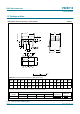
5 Block diagram . . . . . . . . . . . . . . . . . . . . . . . . . . 3
6 Pinning information. . . . . . . . . . . . . . . . . . . . . . 3
6.1 Pinning . . . . . . . . . . . . . . . . . . . . . . . . . . . . . . . 3
6.2 Pin description . . . . . . . . . . . . . . . . . . . . . . . . . 3
7 Functional description . . . . . . . . . . . . . . . . . . . 4
7.1 Sx, Sy: I
2
C-bus SDA or SCL. . . . . . . . . . . . . . . 4
7.2 Lx, Ly: buffered bus LDA or LCL. . . . . . . . . . . . 5
7.3 V
CC
, GND: positive and negative supply pins. . 5
8 Application design-in information . . . . . . . . . . 5
8.1 I
2
C-bus systems . . . . . . . . . . . . . . . . . . . . . . . . 6
8.1.1 Pull-up resistance calculation . . . . . . . . . . . . . . 6
8.1.2 Calculating static bus drive currents . . . . . . . . . 7
8.2 Quick design-in point-to-point/multi-point
circuit information for 5 V bus . . . . . . . . . . . . . 10
8.3 Comparison of P82B715 versus P82B96
in the quick design-in point-to-point/
multi-point circuit. . . . . . . . . . . . . . . . . . . . . . . 11
9 Limiting values. . . . . . . . . . . . . . . . . . . . . . . . . 13
10 Characteristics. . . . . . . . . . . . . . . . . . . . . . . . . 13
11 Test information. . . . . . . . . . . . . . . . . . . . . . . . 14
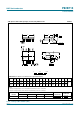
12 Package outline . . . . . . . . . . . . . . . . . . . . . . . . 15
13 Soldering of SMD packages . . . . . . . . . . . . . . 17
13.1 Introduction to soldering . . . . . . . . . . . . . . . . . 17
13.2 Wave and reflow soldering . . . . . . . . . . . . . . . 17
13.3 Wave soldering . . . . . . . . . . . . . . . . . . . . . . . . 17
13.4 Reflow soldering . . . . . . . . . . . . . . . . . . . . . . . 18
14 Soldering of through-hole mount packages . 19
14.1 Introduction to soldering through-hole mount
packages . . . . . . . . . . . . . . . . . . . . . . . . . . . . 19
14.2 Soldering by dipping or by solder wave . . . . . 19
14.3 Manual soldering . . . . . . . . . . . . . . . . . . . . . . 19
14.4 Package related soldering information . . . . . . 20
15 Abbreviations. . . . . . . . . . . . . . . . . . . . . . . . . . 20
16 Revision history. . . . . . . . . . . . . . . . . . . . . . . . 21
17 Legal information. . . . . . . . . . . . . . . . . . . . . . . 22
17.1 Data sheet status . . . . . . . . . . . . . . . . . . . . . . 22
17.2 Definitions. . . . . . . . . . . . . . . . . . . . . . . . . . . . 22
17.3 Disclaimers . . . . . . . . . . . . . . . . . . . . . . . . . . . 22
17.4 Trademarks. . . . . . . . . . . . . . . . . . . . . . . . . . . 22
18 Contact information . . . . . . . . . . . . . . . . . . . . 22
19 Contents. . . . . . . . . . . . . . . . . . . . . . . . . . . . . . 23