
Datasheet


NX3L1T5157 All information provided in this document is subject to legal disclaimers. © NXP B.V. 2011. All rights reserved.
Product data sheet Rev. 6 — 8 November 2011 6 of 21
NXP Semiconductors
NX3L1T5157
Low-ohmic single-pole double-throw analog switch
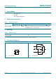
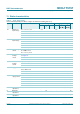
11.1 Test circuits
11.2 ON resistance
V
I
=0.3VorV
CC
0.3 V; V
O
=V
CC
0.3 V or 0.3 V.
Fig 4. Test circuit for measuring OFF-state leakage current
I
S
001aac358
S
Z
Y0
Y1
V
CC
GND
switch
switch
1
1
2
2
V
IL
V
IH
S
V
IL
or V
IH
V
I
V
O
V
I
=0.3VorV
CC
0.3 V; V
O
=V
CC
0.3 V or 0.3 V.
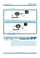
Fig 5. Test circuit for measuring ON-state leakage current
I
S
001aac359
S
Z
Y0
Y1
V
CC
GND
switch
switch
1
1
2
2
V
IL
V
IH
S
V
O
V
IL
or V
IH
V
I
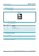
Table 8. ON resistance
At recommended operating conditions; voltages are referenced to GND (ground = 0 V); for graphs see Figure 7
to Figure 13.
Symbol Parameter Conditions T
amb
= 40 C to +85 C T
amb
= 40 C to +125 C Unit
Min Typ
[1]
Max Min Max
R
ON(peak)
ON resistance
(peak)
V
I
=GNDtoV
CC
;
I
SW
= 100 mA; see Figure 6
V
CC
= 1.4 V - 1.6 3.7 - 4.1
V
CC
= 1.65 V - 1.0 1.6 - 1.7
V
CC
= 2.3 V - 0.55 0.8 - 0.9
V
CC
=2.7V - 0.5 0.75 - 0.9
V
CC
=4.3V - 0.5 0.75 - 0.9