
Datasheet


NX3L1T5157 All information provided in this document is subject to legal disclaimers. © NXP B.V. 2011. All rights reserved.
Product data sheet Rev. 6 — 8 November 2011 12 of 21
NXP Semiconductors
NX3L1T5157
Low-ohmic single-pole double-throw analog switch
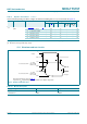
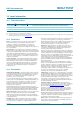
a. Test circuit
b. Input and output measurement points
Fig 15. Test circuit for measuring break-before-make timing
001aag571
GND
V
CC
V
EXT
= 1.5 V
Y0
Y1
S
Z
V
I
V
V
O
R
L
C
L
G
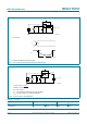
001aag572
V
I
t
b-m
V
O
0.9V
O
0.9V
O
0.5V
I
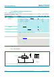
Test data is given in Table 11.
Definitions test circuit:
R
L
= Load resistance.
C
L
= Load capacitance including jig and probe capacitance.
V
EXT
= External voltage for measuring switching times.
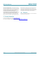
Fig 16. Load circuit for switching times
001aag642
S
Z
Y0
Y1
R
L
C
L
V
CC
GND
V
EXT
= 1.5 V
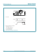
switch
1
2
V
I
V
V
O
G
Table 11. Test data
Supply voltage Input Load
V
CC
V
I
t
r
, t
f
C
L
R
L
1.4 V to 4.3 V V
CC
2.5ns 35pF 50