
Datasheet


NX3L1G384 All information provided in this document is subject to legal disclaimers. © NXP B.V. 2012. All rights reserved.
Product data sheet Rev. 6 — 3 July 2012 9 of 18
NXP Semiconductors
NX3L1G384
Low-ohmic single-pole single-throw analog switch
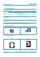
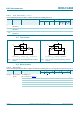
12.1 Waveform and test circuits
Measurement points are given in Table 10.
Logic level: V
OH
is the typical output voltage that occurs with the output load.
Fig 15. Enable and disable times
001aai600
t
en
t
dis
switch
enabled
switch
disabled
switch
disabled
V
X
V
X
Y or Z output
LOW to OFF
OFF to LOW
E input
GND
V
OH
V
M
V
M
GND
V
I
Table 10. Measurement points
Supply voltage Input Output
V
CC
V
M
V
X
1.4 V to 4.3 V 0.5V
CC
0.9V
OH
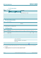
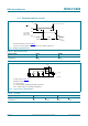
Test data is given in Table 11.
Definitions test circuit:
R
L
= load resistance.
C
L
= load capacitance including jig and probe capacitance.
V
EXT
= external voltage for measuring switching times.
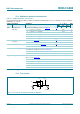
Fig 16. Load circuit for switching times
VV
I
V
O
001aai601
C
L
R
L
Y/Z Z/Y
E
V
CC
V
EXT
= 1.5 V
G
Table 11. Test data
Supply voltage Input Load
V
CC
V
I
t
r
, t
f
C
L
R
L
1.4 V to 4.3 V V
CC
2.5ns 35pF 50