
Datasheet


NX3L1G384 All information provided in this document is subject to legal disclaimers. © NXP B.V. 2012. All rights reserved.
Product data sheet Rev. 6 — 3 July 2012 6 of 18
NXP Semiconductors
NX3L1G384
Low-ohmic single-pole single-throw analog switch
[1] Typical values are measured at T
amb
= 25 C.
[2] Flatness is defined as the difference between the maximum and minimum value of ON resistance measured at identical V
CC
and
temperature.
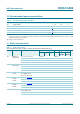
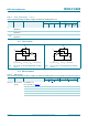
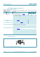
11.3 ON resistance test circuit and graphs
R
ON(flat)
ON resistance
(flatness)
V
I
=GNDtoV
CC
;
I
SW
=100mA
[2]
V
CC
= 1.4 V - 1.0 3.3 - 3.6
V
CC
= 1.65 V - 0.5 1.2 - 1.3
V
CC
= 2.3 V - 0.15 0.3 - 0.35
V
CC
= 2.7 V - 0.13 0.3 - 0.35
V
CC
= 4.3 V - 0.2 0.4 - 0.45
Table 8. ON resistance …continued
At recommended operating conditions; voltages are referenced to GND (ground = 0 V); for graphs see Figure 8 to Figure 14.
Symbol Parameter Conditions T
amb
= 40 C to +85 C T
amb
= 40 C to +125 C Unit
Min Typ
[1]
Max Min Max
R
ON
=V
SW
/ I
SW
.(1)V
CC
=1.5V.
(2) V
CC
=1.8V.
(3) V
CC
=2.5V.
(4) V
CC
=2.7V.
(5) V
CC
=3.3V.
(6) V
CC
=4.3V.
Measured at T
amb
=25C.
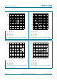
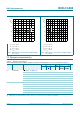
Fig 7. Test circuit for measuring ON resistance Fig 8. Typical ON resistance as a function of input
voltage
001aai599
Z
E
V
IL
Y
GND
V
CC
V
l
V
SW
I
SW
V
V
I
(V)
054312
001aag564
0.8
0.4
1.2
1.6
R
ON
(Ω)
0
(1)
(2)
(5)
(6)
(4)
(3)