
Datasheet

NX3DV42 All information provided in this document is subject to legal disclaimers. © NXP B.V. 2013. All rights reserved.
Product data sheet Rev. 3 — 13 February 2013 9 of 19
NXP Semiconductors
NX3DV42
Dual high-speed USB 2.0 double-pole double-throw analog switch
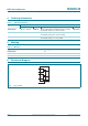
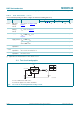
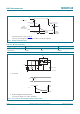
Measurement points are given in Table 10.
Logic level: V
OH
is the typical output voltage level that occurs with the output load.
Fig 11. Enable and disable times
aaa-001361
t
PHZ
switch
disabled
switch
enabled
switch
enabled
output
HIGH to OFF
OFF to HIGH
S, OE input
V
OH
GND
GND
V
I
t
PZH
V
M
V
X
V
X
Table 10. Measurement points
Supply voltage Input Output
V
CC
V
M
V
I
V
X
3.0 V to 3.6 V 0.5V
CC
V
CC
0.9V
OH
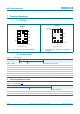
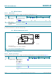
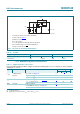
a. Test circuit.
b. Input and output measurement points.
Test circuit also applies for D+, HSD1+ and HSD2+.
Fig 12. Test circuit for measuring break-before-make timing
aaa-001364
R
L
V
O
S
GND
OE
D-
V
CC
V
I
V
IL
C
L
G
V
EXT
= 0.8 V
HSD1-
HSD2-
V
001aag572
V
I
t
b-m
V
O
0.9V
O
0.9V
O
0.5V
I